> For the complete documentation index, see [llms.txt](https://docs.hackerfab.org/home/llms.txt). Markdown versions of documentation pages are available by appending `.md` to page URLs; this page is available as [Markdown](https://docs.hackerfab.org/home/fab-toolkit/electronic-design-automation/magicvlsi-drc-and-lvs-wip.md).
# MagicVLSI DRC and LVS - WIP
MagicVLSI is an open-source EDA tool capable of real-time DRC detection, generating SPICE (Simulation Program with Integrated Circuit Emphasis) netlist, and more.
## Getting Started with Magic
Note: By convention and for simplicity, MagicVLSI will be referred to as Magic in this documentation.
First, read over the official documentation of [Magic](http://opencircuitdesign.com/magic/).
There are two ways to use Magic: by installing it directly and by cloning it through [GitHub ](https://github.com/RTimothyEdwards/magic)and running it through your terminal. The second method is usually preferred as you have an easier time updating this version (through updates using GitHub).
Below, a method to run Magic through GitHub in a Linux-based environment is presented. WSL (Windows Subsystem for Linux) compatible. For more information on how to run a Linux-based environment on a Windows device, check "[How to install Linux on Windows with WSL](https://learn.microsoft.com/en-us/windows/wsl/install)."
First, update the system and install a graphical interface
```
sudo apt update && sudo apt upgrade
sudo apt install m4 tcl-dev tk-dev libx11-dev tcsh csh
```
Next, clone the official GitHub repository (create a GitHub account first and link your account to the terminal - for more instructions, see the [GitHub Docs](https://docs.github.com/en/get-started/git-basics/set-up-git)):
```
git clone https://github.com/RTimothyEdwards/magic.git
```
The terminal should display something similar to this (do not type this into your terminal):
```
Cloning into 'magic'...
remote: Enumerating objects: 18948, done.
remote: Counting objects: 100% (2861/2861), done.
remote: Compressing objects: 100% (409/409), done.
remote: Total 18948 (delta 2520), reused 2453 (delta 2451), pack-reused 16087 (from 2)
Receiving objects: 100% (18948/18948), 10.95 MiB | 4.09 MiB/s, done.
Resolving deltas: 100% (12790/12790), done.
Updating files: 100% (1292/1292), done.
```
After "magic" finishes cloning into your folder:
```
cd magic
```
```
./configure
make
sudo make install
```
Now, running magic in your terminal, the layout and prompt screen should both pop up on screen, and the most basic version of magic is now running on your device!
```
magic
```
## PDK (Process Design Kit)
To actually make Magic useful, a PDK is required; this is basically a set of models, design rules, device characteristics, and materials that tell the EDA software what is available and what can be used. Usually, a PDK is a collection of foundry-supplied files; however, Hackerfab's goal lies in the creation of a foundry, and thus, *the PDK must be determined, created, and verified by each individual lab based on their specific materials, device characteristics, and capabilities.*
Since this is a difficult process, we can first utilize the PDKs already developed by other foundries that are open-sourced to draw layers, test out ideas, and create masks; this is possible through the GitHub OpenPDK:
First, make sure to cd out of your magic directory, then:
```
git clone https://github.com/RTimothyEdwards/open_pdks.git
cd open_pdks
```
Here, the [SKY130 PDK](https://skywater-pdk.readthedocs.io/en/main/) will be used. This is an open-source 130 nm CMOS Process Design Kit (PDK) released by SkyWater Technology, Efabless, and Google, and is one of (if not) the most popular PDKs in the open-source community.
```
./configure --enable-sky130-pdk
```
```
make -j$(nproc)
sudo make install
```
NOTE!!! Before you run the step above, this will take a significant amount of time (\~hours), and space in your device, as PDKs are massive, and this contains multiple. Also note that the -j$(nproc) flag runs all your CPU cores together in parallel to speed up the process; if you want to limit CPU use, remove the -j flag.
Then, create a folder for SKY130. In this folder, every time you run magic, you will run it in conjunction with the SKY130 PDK
```
mkdir sky130_design
cd sky130_design
cp /usr/local/share/pdk/sky130A/libs.tech/magic/sky130A.magicrc .magicrc
```
After running these scripts, you should see a .magicrc file being copied into your new folder. This file is recognized each time "magic" runs, and acts as a startup script for the application, responsible for the .tech file (the magic equivalent of PDK) and the interface.
Below is what the .magicrc file is supposed to look like:
```
puts stdout "Sourcing design .magicrc for technology sky130A ..."
# Put grid on 0.005 pitch. This is important, as some commands don't
# rescale the grid automatically (such as lef read?).
set scalefac [tech lambda]
if {[lindex $scalefac 1] < 2} {
scalegrid 1 2
}
# drc off
drc euclidean on
# Change this to a fixed number for repeatable behavior with GDS writes
# e.g., "random seed 12345"
catch {random seed}
# Turn off the scale option on ext2spice or else it conflicts with the
# scale in the model files.
ext2spice scale off
# Allow override of PDK path from environment variable PDK_ROOT
# "file nativename" guards against a local PDK_ROOT with "~" in the name
if {[catch {set PDK_ROOT [file nativename $env(PDK_ROOT)]}]} {
set PDK_ROOT /usr/local/share/pdk
}
# loading technology
tech load $PDK_ROOT/sky130A/libs.tech/magic/sky130A.tech
# halt on error
if {[tech name] != "sky130A"} {quit -noprompt}
# load device generator
source $PDK_ROOT/sky130A/libs.tech/magic/sky130A.tcl
# load bind keys (optional)
# source $PDK_ROOT/sky130A/libs.tech/magic/sky130A-BindKeys
# set units to lambda grid
snap lambda
# set sky130 standard power, ground, and substrate names
set VDD VPWR
set GND VGND
set SUB VSUBS
# Allow override of type of magic library views used, "mag" or "maglef",
# from environment variable MAGTYPE
if {[catch {set MAGTYPE $env(MAGTYPE)}]} {
set MAGTYPE mag
}
# add path to reference cells
addpath ${PDK_ROOT}/sky130A/libs.ref/sky130_fd_pr/${MAGTYPE}
addpath ${PDK_ROOT}/sky130A/libs.ref/sky130_fd_io/${MAGTYPE}
addpath ${PDK_ROOT}/sky130A/libs.ref/sky130_fd_sc_hd/${MAGTYPE}
addpath ${PDK_ROOT}/sky130A/libs.ref/sky130_fd_sc_hdll/${MAGTYPE}
addpath ${PDK_ROOT}/sky130A/libs.ref/sky130_fd_sc_hs/${MAGTYPE}
addpath ${PDK_ROOT}/sky130A/libs.ref/sky130_fd_sc_hvl/${MAGTYPE}
addpath ${PDK_ROOT}/sky130A/libs.ref/sky130_fd_sc_lp/${MAGTYPE}
addpath ${PDK_ROOT}/sky130A/libs.ref/sky130_fd_sc_ls/${MAGTYPE}
addpath ${PDK_ROOT}/sky130A/libs.ref/sky130_fd_sc_ms/${MAGTYPE}
addpath ${PDK_ROOT}/sky130A/libs.ref/sky130_osu_sc/${MAGTYPE}
addpath ${PDK_ROOT}/sky130A/libs.ref/sky130_osu_sc_t18/${MAGTYPE}
addpath ${PDK_ROOT}/sky130A/libs.ref/sky130_ml_xx_hd/${MAGTYPE}
addpath ${PDK_ROOT}/sky130A/libs.ref/sky130_fd_bd_sram/${MAGTYPE}
addpath ${PDK_ROOT}/sky130A/libs.ref/sky130_sram_macros/${MAGTYPE}
```
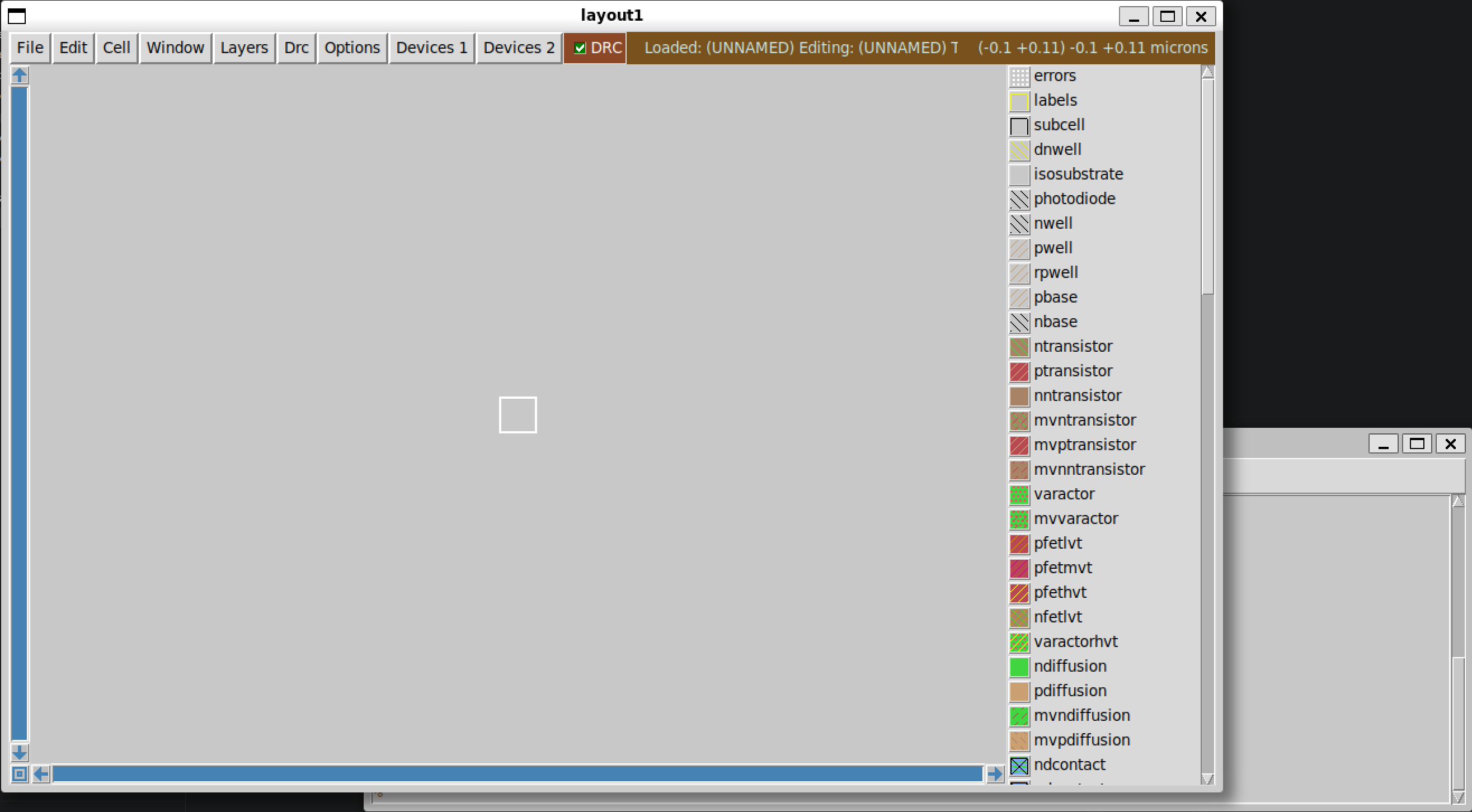
Now run "magic" again in your terminal (while inside the sky130\_design folder), the Magic layout tool and prompt should pop up again with more materials/elements on the side, such as "nwell", "pwell", ... Then you have integrated a fully functional MagicVLSI with the SKY130 PDK and can start your design process!
Should look something similar to this:
## PDK, DRC, LVS, and the .tech file
Below are the steps developed to create an LVS (Layout vs. Schematic) standard process using MagicVLSI. Including the use of Netgen, Xschem, and the process of creating your own PDK (.tech) file in magic, as well as creating interactive User Interface windows using the .magicrc file.
#### Background:
Before starting this process, it is important to understand the relationships between these acronyms. PDK stands for *Process Design Kit* and has been introduced in the previous section.
DRC stands for *Design Rule Check;* design rules are usually rules dictated by the fab (foundry) to make sure the chip that has been designed in an EDA tool is actually manufacturable and will have a relatively good yield rate. Some examples of design rules are the minimum width of a material (PolySi, N-Diffusion,...), the minimum spacing. Check the [Synopsys guide](https://www.synopsys.com/glossary/what-is-design-rule-checking.html) for more information. Design rules are usually integrated as part of the PDK, and Magic will constantly check for violations through the live DRC feature.
No Errors, as you can see from the DRC=0 and green checkmark on top.
You can see that there are DRC violations here, as DRC is not 0, and the checkmark becomes red. Using the command "drc why" in the Magic terminal while highlighting the spots with white dots (meaning drc violation), you can see the reason for the error:
Here it states:
```
-- Diffusion width < 0.15um (diff/tap.1)
```
Meaning the width of the n-diffusion is too small and needs to be expanded.
[Layout Versus Schematic](https://www.synopsys.com/glossary/what-is-layout-versus-schematic-checking.html) (LVS) compares the extracted netlist from the layout (with physical layers and specific materials) to the original schematic netlist (similar to a circuit diagram with specifications) to determine if they match. The comparison check is considered clean if all the devices and nets of the schematic match the devices and the nets of the layout. In more advanced comparisons, LVS will compare the device characteristics to see if they fit within the accepted tolerances. This is through generating a SPICE (Simulation Program with Integrated Circuit Emphasis) netlist using the layout tool and the schematic tool. This is similar to a textual or mathematical representation of the circuit. Below are two examples of SPICE netlists based on the SKY130 PDK:
A standard 1.8V NMOS in Magic exported as a SPICE netlist:
```
** sch_path: /___/_/___/_____/HackerFab_NMOS_EDA/untitled.sch
.subckt untitled D S G B
*.PININFO D:B S:B G:I B:I
XM1 D G S B sky130_fd_pr__nfet_01v8 L=0.42 W=0.42 nf=1
.ends
```
A standard 1.8V NMOS in Xschem (a schematic creation tool) exported as a SPICE netlist:
```
* NGSPICE file created from layout1.ext - technology: sky130A
.subckt sky130_fd_pr__nfet_01v8_SDTWRA B D S G
X0 S G D B sky130_fd_pr__nfet_01v8 ad=0.1218 pd=1.42 as=0.1218 ps=1.42 w=0.42 l=0.42
.ends
.subckt layout1
Xsky130_fd_pr__nfet_01v8_SDTWRA_0 VSUBS sky130_fd_pr__nfet_01v8_SDTWRA_0/D sky130_fd_pr__nfet_01v8_SDTWRA_0/S
+ sky130_fd_pr__nfet_01v8_SDTWRA_0/G sky130_fd_pr__nfet_01v8_SDTWRA
.ends
```
An LVS checking between these two SPICE netlists using Netgen looks like this:
```
Circuit 1 cell sky130_fd_pr__nfet_01v8 and Circuit 2 cell sky130_fd_pr__nfet_01v8 are black boxes.
Warning: Equate pins: cell sky130_fd_pr__nfet_01v8 is a placeholder, treated as a black box.
Warning: Equate pins: cell sky130_fd_pr__nfet_01v8 is a placeholder, treated as a black box.
Subcircuit pins:
Circuit 1: sky130_fd_pr__nfet_01v8 |Circuit 2: sky130_fd_pr__nfet_01v8
-------------------------------------------|-------------------------------------------
1 |1
2 |2
3 |3
4 |4
---------------------------------------------------------------------------------------
Cell pin lists are equivalent.
Device classes sky130_fd_pr__nfet_01v8 and sky130_fd_pr__nfet_01v8 are equivalent.
Subcircuit summary:
Circuit 1: sky130_fd_pr__nfet_01v8_SDTWRA |Circuit 2: untitled
-------------------------------------------|-------------------------------------------
sky130_fd_pr__nfet_01v8 (1) |sky130_fd_pr__nfet_01v8 (1)
Number of devices: 1 |Number of devices: 1
Number of nets: 4 |Number of nets: 4
---------------------------------------------------------------------------------------
Resolving symmetries by property value.
Resolving symmetries by pin name.
Netlists match uniquely.
Subcircuit pins:
Circuit 1: sky130_fd_pr__nfet_01v8_SDTWRA |Circuit 2: untitled
-------------------------------------------|-------------------------------------------
G |G
D |D
S |S
B |B
---------------------------------------------------------------------------------------
Cell pin lists are equivalent.
Device classes sky130_fd_pr__nfet_01v8_SDTWRA and untitled are equivalent.
Final result: Circuits match uniquely.
.
```
The final line is the most important: "Final result: Circuits match uniquely." This is the best thing to see, though obvious, it holds true in this case as the two circuits are simple NMOSes with the same dimensions.
---
# Agent Instructions
This documentation is published with GitBook. GitBook is the documentation platform designed so that both humans and AI agents can read, navigate, and reason over technical content effectively. Learn more at gitbook.com.
## Querying This Documentation
If you need additional information that is not directly available in this page, you can query the documentation by asking a question.
Perform an HTTP GET request on the following URL with the `ask` and `goal` query parameters:
```
GET https://docs.hackerfab.org/home/fab-toolkit/electronic-design-automation/magicvlsi-drc-and-lvs-wip.md?ask=&goal=
```
`ask` is the immediate question: it should be specific, self-contained, and written in natural language.
`goal` is what the user is ultimately trying to achieve, the reason they need the answer. Sharing it helps GitBook give you a better, more relevant answer. A goal is most helpful when it describes the outcome the user wants rather than restating the question. For example, with `ask=how do I create an API token`, a goal like `automate deployments from our CI pipeline` lets GitBook tailor the answer to that use case.
The response will contain a direct answer to the question and relevant excerpts and sources from the documentation.
Use this mechanism when the answer is not explicitly present in the current page, you need clarification or additional context, or you want to retrieve related documentation sections.