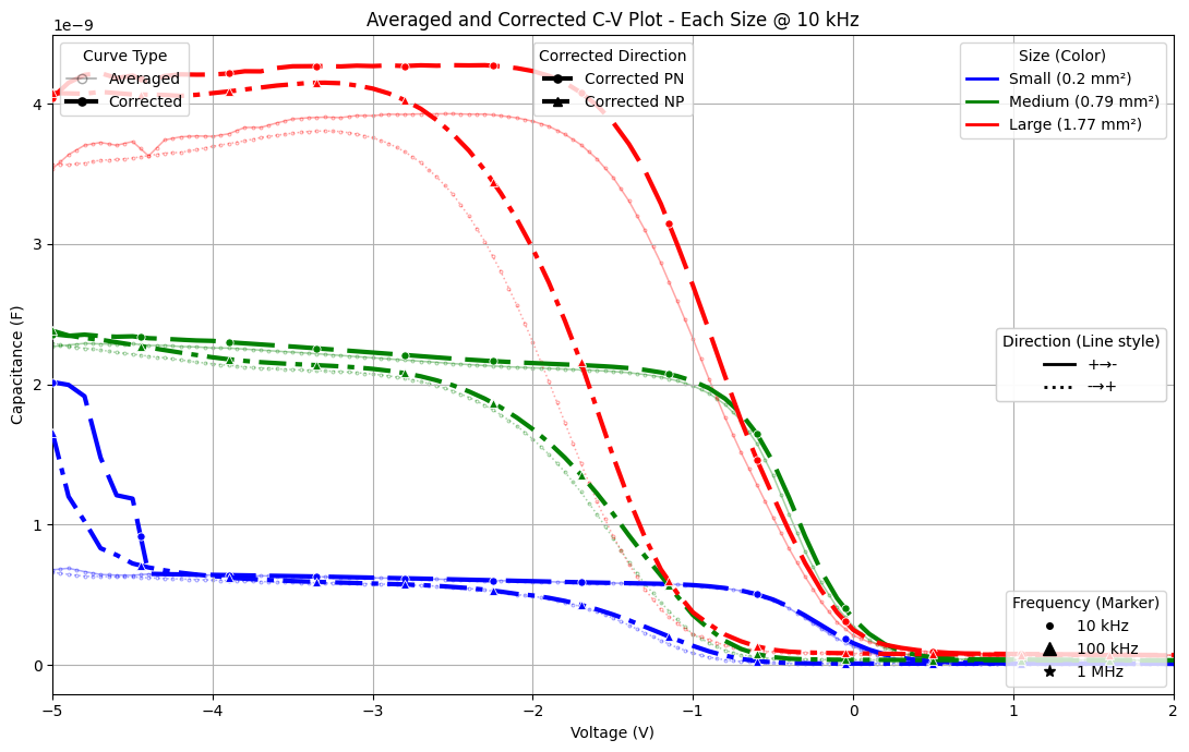
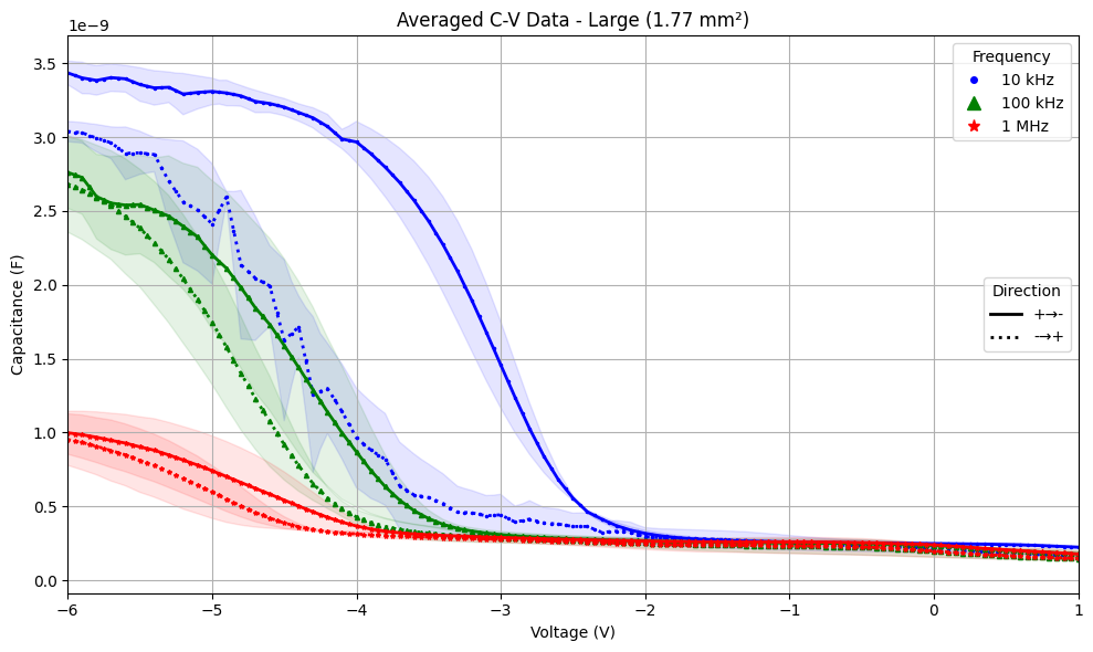
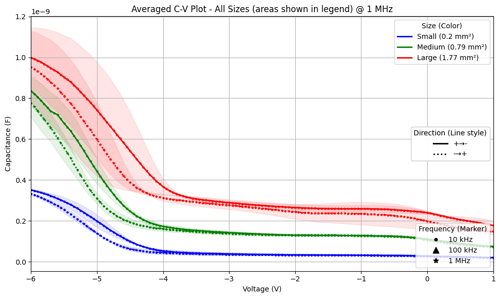
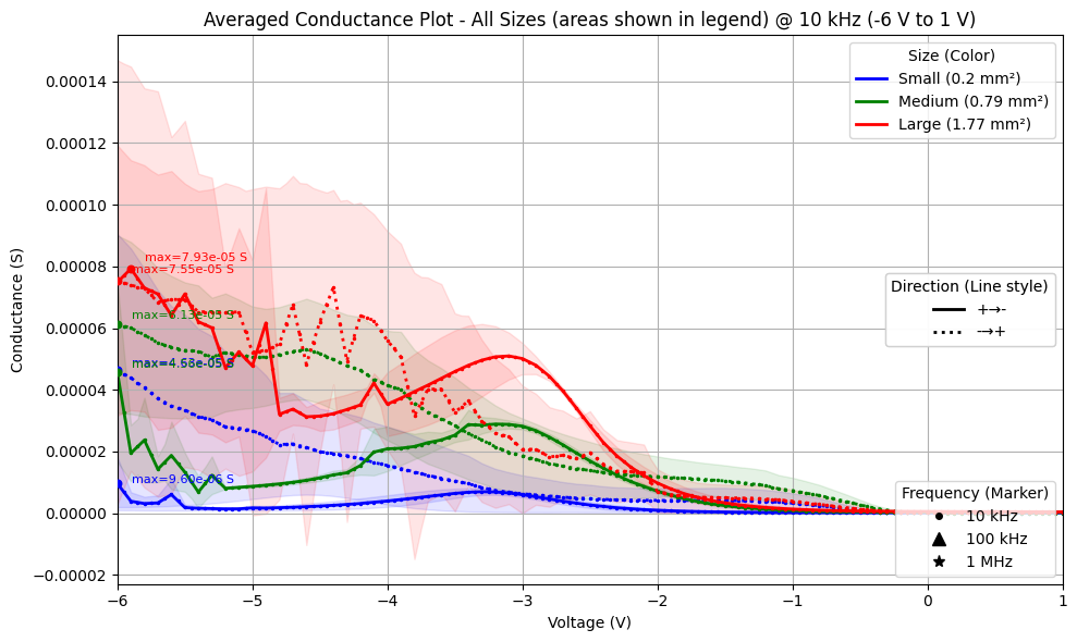
| Step # | Step Name | Parameters | Layer Stacks |
|---|---|---|---|
| 0 | Substrate Stack | Si p-type 5-10 ohms (100): 525 µm | |
| 1 | RCA Clean | SC 1 Constituents: H2O:NH4OH(29%):H2O2(30%) (5:1:1) SC 1 Cleaning Time: 10 mins SC 1 Cleaning Temperature: 80 °C HF Concentration: 6:1 BOE HF Dip Time: 15 secs HF Dip Temperature: 20 °C SC 2 Constituents: H2O:HCl(37%):H2O2(30%) (6:1:1) SC 2 Cleaning Time: 10 mins SC 2 Cleaning Temperature: 80 °C "SC 1 and 2 mixed in 50ml pyrex beakers directly before using. Optional HF last processing step (Experimental Option) Rinsed with DI Water then N2 dried. Immediately placed into sputtering chamber for pump down." | |
| 2 | Sputter w/ CMU Hacker Fab RF Sputtering Chamber | Material: Al2O3 Film thickness: Experimental Option Deposition Rate: .00025 µm/min Deposition Time: 80 mins Sputter Type: RF Sputtering RF or DC Power: 100 Watts Sputter Gas Composition: 9 SCCM UHP Ar : 9 SCCM UHP O2 Chamber Pressure: 4.7E-3 Torr Throw Distance: 3" Base Pressure Pre Deposition: 1E-7 Torr Target Sputter Clean Ar Flow: 30 SCCM Target Sputter Clean Time: 15 Minutes | |
| 3 | Anneal (Experimental Option) | Performed in RF sputtering Chamber under partial Vacuum. Pump speed at 250Hz with 50 SCCM of either UHP Ar or UHP O2. | |
| 4 | Sputter w/ CMU Hacker Fab RF Sputtering Chamber | Material: Al Film thickness: 150 nm Deposition Rate: .0025 µm/min Deposition Time: 60 mins Sputter Type: RF Sputtering RF or DC Power: 100 Watts Sputter Gas Composition: 15 SCCM UHP Ar Chamber Pressure: 3E-3 Torr Throw Distance: 3" Base Pressure Pre Deposition: 1E-7 Torr Target Sputter Clean Ar Flow: 30 SCCM Target Sputter Clean Time: 15 Minutes SWR During Deposition: 1.5 | |
| 6 | Sputter w/ CMU Hacker Fab RF Sputtering Chamber | Material: Al Film thickness: 150 nm Deposition Rate: .0025 µm/min Deposition Time: 60 mins Sputter Type: RF Sputtering RF or DC Power: 100 Watts Sputter Gas Composition: 15 SCCM UHP Ar Chamber Pressure: 3E-3 Torr Throw Distance: 3" Base Pressure Pre Deposition: 1E-7 Torr Target Sputter Clean Ar Flow: 30 SCCM Target Sputter Clean Time: 15 Minutes SWR During Deposition: 1.5 | |


.png?alt=media&token=8e109c04-ad45-4d02-85ef-b6e59477371b)
.png?alt=media&token=d8dfcf28-fe45-4901-b4f2-86b7929a0968)
| Step # | Step Name | Parameters | Layer Stacks |
|---|---|---|---|
| 0 | Substrate Stack | p-Si 5-10 ohm (100): 525 µm |  |
| 1 | Acetone + IPA Clean (N2 dry) | Cleaning Agent: Acetone then IPA Squirt with Acetone, then IPA, then dry the surface with the N2 gun. | |
| 2 | Bake | Bake Temperature: 100 °C Bake Time: 60 secs | |
| 3 | Spin-Coat | Material Type: Adhesion Promoter Material: HMDS Spin Speed: 4000 rpm Spin Time: 30 secs | |
| 4 | Bake | Bake Temperature: 100 °C Bake Time: 60 secs | |
| 5 | Spin Resist | Resist: AZ P4210 Resist Type: Positive Spin Speed: 4000 rpm Spin Time: 30 secs |  |
| 6 | Bake | Bake Temperature: 100 °C Bake Time: 90 secs | |
| 7 | Hacker Fab Maskless Litho Stepper | Exposure time: 8 secs |  |
| 8 | Develop | Developer: AZ 400K : DI Water (1:3) Develop Time: 30 secs |  |
| 9 | Wet-Etch | Actually performed with SF6 RIE, but can be replaced by a Nitric + HF wet etch solution since this step simply creates alignment marks in the Si. |  |
| 10 | Wet Strip Resist | Stripping Agent(s): Acetone then IPA Blow dry with N2 gun after. |  |
| 11 | RCA Clean | SC 1 Constituents: H2O:NH4OH(29%):H2O2(30%) (5:1:1) SC 1 Cleaning Time: 10 mins SC 1 Cleaning Temperature: 80 °C HF Concentration: 6:1 BOE HF Dip Time: 15 secs HF Dip Temperature: 20 °C SC 2 Constituents: H2O:HCl(37%):H2O2(30%) (6:1:1) SC 2 Cleaning Time: 10 mins SC 2 Cleaning Temperature: 80 °C | |
| 12 | Spin-Coat | Material Type: Non-Resist Material: 700B (spin on glass) Spin Speed: 4000 rpm Spin Time: 20 secs |  |
| 13 | Bake | Bake Temperature: 400 °C Bake Time: 10 mins | |
| 14 | Spin-Coat | Material Type: Adhesion Promoter Material: HMDS Spin Speed: 4000 rpm Spin Time: 30 secs | |
| 15 | Bake | Bake Temperature: 100 °C Bake Time: 60 secs | |
| 16 | Spin Resist | Resist: AZ P4210 Resist Type: Positive Spin Speed: 4000 rpm Spin Time: 30 secs |  |
| 17 | Bake | Bake Temperature: 100 °C Bake Time: 90 secs | |
| 18 | Hacker Fab Maskless Litho Stepper | Exposure time: 8 secs |  |
| 19 | Develop | Developer: AZ 400K : DI Water (1:3) Develop Time: 30 secs |  |
| 20 | Wet-Etch | Etch Time: 20 secs Etching Agent(s): 6:1 BOE |  |
| 21 | Wet Strip Resist | Stripping Agent(s): Acetone then IPA Blow dry with N2 gun after. |  |
| 22 | Spin-On Dopant | Spin-On Dopant Name: P504 (Phosphorus source) Spin Speed: 4000 rpm Spin Time: 20 secs |  |
| 23 | Bake | Bake Temperature: 200 °C Bake Time: 10 mins | |
| 24 | Dopant Diffusion | Diffusion Time: 30 mins Diffusion Temperature: 1100 °C Environmental: false |  |
| 25 | Wet-Etch | Etch Time: 10 mins Etching Agent(s): 6:1 BOE |  |
| 26 | RCA Clean | SC 1 Constituents: H2O:NH4OH(29%):H2O2(30%) (5:1:1) SC 1 Cleaning Time: 10 mins SC 1 Cleaning Temperature: 80 °C HF Concentration: 6:1 BOE HF Dip Time: 15 secs HF Dip Temperature: 20 °C SC 2 Constituents: H2O:HCl(37%):H2O2(30%) (6:1:1) SC 2 Cleaning Time: 80 mins SC 2 Cleaning Temperature: 75 °C | |
| 27 | Sputter w/ CMU Hacker Fab RF Sputtering Chamber | Material: Al2O3 Film thickness: 20 nm Deposition Rate: .25 Å/s Deposition Time: 80 mins Sputter Type: RF Sputtering RF or DC Power: 100 Watts Sputter Gas Composition: 9 SCCM UHP Ar : 9 SCCM UHP O2 Chamber Pressure: 4.7E-3 Torr Throw Distance: 3" Base Pressure Pre Deposition: 1E-7 Torr Target Sputter Clean Ar Flow: 30 SCCM Target Sputter Clean Time: 15 Minutes SWR During Deposition: 1.5 |  |
| 28 | Sputter w/ CMU Hacker Fab RF Sputtering Chamber | Material: Al Film thickness: 150 nm Deposition Rate: 2.5 Å/s Deposition Time: 60 mins Sputter Type: RF Sputtering RF or DC Power: 100 Watts Sputter Gas Composition: 15 SCCM UHP Ar Chamber Pressure: 3E-3 Torr Throw Distance: 3" Base Pressure Pre Deposition: 1E-7 Torr Target Sputter Clean Ar Flow: 30 SCCM Target Sputter Clean Time: 15 Minutes SWR During Deposition: 1.5 |  |
| 29 | Spin Resist | Resist: AZ P4210 Resist Type: Positive Spin Speed: 4000 rpm Spin Time: 30 secs |  |
| 30 | Bake | Bake Temperature: 100 °C Bake Time: 90 secs | |
| 31 | Hacker Fab Maskless Litho Stepper | Exposure time: 8 secs |  |
| 32 | Develop | Developer: AZ 400K : DI Water (1:3) Develop Time: 30 secs |  |
| 33 | Wet-Etch | Etch Time: 8 mins Etching Agent(s): Type A Al Etch (PAN) Etch Temperature: 40 °C |  |
| 34 | Wet Strip Resist | Stripping Agent(s): Acetone then IPA Blow dry with N2 gun after. |  |
| 35 | Spin-Coat | Material Type: Non-Resist Material: 700B (spin on glass) Spin Speed: 4000 rpm Spin Time: 20 secs |  |
| 36 | Bake | Bake Temperature: 400 °C Bake Time: 10 mins | |
| 37 | Spin-Coat | Material Type: Adhesion Promoter Material: HMDS Spin Speed: 4000 rpm Spin Time: 30 secs | |
| 38 | Bake | Bake Temperature: 100 °C Bake Time: 60 secs | |
| 39 | Spin Resist | Resist: AZ P4210 Resist Type: Positive Spin Speed: 4000 rpm Spin Time: 30 secs |  |
| 40 | Bake | Bake Temperature: 100 °C Bake Time: 90 secs | |
| 41 | Hacker Fab Maskless Litho Stepper | Exposure time: 8 secs |  |
| 42 | Develop | Developer: AZ 400K : DI Water (1:3) Develop Time: 30 secs |  |
| 43 | Wet-Etch | Etch Time: 20 secs Etching Agent(s): 6:1 BOE |  |
| 44 | Wet Strip Resist | Stripping Agent(s): Acetone then IPA Blow dry with N2 gun after. |  |
| 45 | Sputter w/ CMU Hacker Fab RF Sputtering Chamber | Material: Al Film thickness: 300 nm Deposition Rate: 2.5 Å/s Deposition Time: 120 mins Sputter Type: RF Sputtering RF or DC Power: 100 Watts Sputter Gas Composition: 15 SCCM UHP Ar Chamber Pressure: 3E-3 Torr Throw Distance: 3" Base Pressure Pre Deposition: 1E-7 Torr Target Sputter Clean Ar Flow: 30 SCCM Target Sputter Clean Time: 15 Minutes SWR During Deposition: 1.5 |  |
| 46 | Spin Resist | Resist: AZ P4210 Resist Type: Positive Spin Speed: 4000 rpm Spin Time: 30 secs |  |
| 47 | Bake | Bake Temperature: 100 °C Bake Time: 90 secs |  |
| 48 | Hacker Fab Maskless Litho Stepper | Exposure time: 8 secs |  |
| 49 | Develop | Developer: AZ 400K : DI Water (1:3) Develop Time: 30 secs |  |
| 50 | Wet-Etch | Etch Time: 4 mins Etching Agent(s): Type A Al Etchant (PAN) |  |
| 51 | Wet Strip Resist | Stripping Agent(s): Acetone then IPA Blow dry with N2 gun after. |  |
.png?alt=media&token=6fbf4526-1136-4c2e-b596-ac7225e59cbd)
.png?alt=media&token=75a17aaa-05f7-48ea-a140-45de26d19289)
.png?alt=media&token=6986850b-4704-4493-b9b5-39fe0908ed9a)
.png?alt=media&token=71a56df1-2d88-4c25-a5fb-c3d2f67dda38)
.png?alt=media&token=5519a1a7-76cd-4725-bd21-4f4bdfe8e0b9)
.png?alt=media&token=7f759c26-e0c5-4c52-8997-62353f5810e6)
.png?alt=media&token=805c65f8-9145-4eeb-81e3-4b104a760ee6)
.png?alt=media&token=ea772b3d-d6e0-46e2-a53b-df9ab2bd1005)
.png?alt=media&token=68e49b88-b101-4243-9e60-da5a6a0f0e6b)
.png?alt=media&token=ff837463-006f-49a1-b320-a96659f470cd)
.png?alt=media&token=faeebd54-09d4-4e4a-a68e-2ab69a35a403)


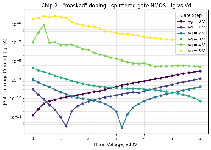


| Chip/Processing | On Current Vd=5, Vg=0 (A) | Off Current Vd=5, Vg=0 (A) | On/Off Ratio Vd = 5 | Gate Leakage at Vg=Vd=5V (A) |
|---|---|---|---|---|
| pre anneal | 4.4E-4 | 1.2E-6 | 369 | 1.45e-7 |
| 400C open air anneal | 4.9E-4 | 2.2E-6 | 227 | 4e-5 |
RF Sputtering with Al2O3 target, 1% O2, 99% Ar, 20sccm totla flow
30nm thick Al2O3
 |
| -------------------------------------------------------------------------------------------- | --------------------------------------------------------------------------------------------------------------------------------------------------------------------------------------------------------------------------------------------------------- |
|
|
| -------------------------------------------------------------------------------------------- | --------------------------------------------------------------------------------------------------------------------------------------------------------------------------------------------------------------------------------------------------------- |
| Al Thermal Evaporation
300nm thick Al
 |
The NMOS also had step 24 modified to be 5 min at 1100C instead of 30min.
The PMOS chip had step 22 modified to use B154 the Boron SOD from filmtronics. Additionally step 24 modified to be 5 min at 1000C due to higher mobility of Boron.
PMOS and NMOS Images and Testing Results
|
The NMOS also had step 24 modified to be 5 min at 1100C instead of 30min.
The PMOS chip had step 22 modified to use B154 the Boron SOD from filmtronics. Additionally step 24 modified to be 5 min at 1000C due to higher mobility of Boron.
PMOS and NMOS Images and Testing Results


.png?alt=media&token=12ca045c-ceb6-46b3-bd2d-b824e498b801)
.png?alt=media&token=e0d43dfd-bfba-4de9-ab06-f2ce3ce23101)
.png?alt=media&token=2ec16801-dd9e-420e-9a06-71af720c8440)
.png?alt=media&token=e30180a1-2451-456e-83ca-07a6817b8cba)
.png?alt=media&token=6a7ea47c-9c8c-4bf2-8847-f0e1a3a30062)
.png?alt=media&token=c28244ba-20a7-4eb5-b3c9-edc59c653396)
| Chip | On Current Vd=5, Vg=0 (A) | Off Current Vd=5, Vg=0 (A) | On/Off Ratio Vd = 5 | Gate Leakage at Vg=Vd=5V (A) |
|---|---|---|---|---|
| PMOS | 2.45e-4 | 3.96e-7 | 617.9 | 9e-10 |
| NMOS | 1.5e-3 | 5.6e-5 | 26.3 | 1.2e-8 |

.png?alt=media&token=704d979a-e02d-42db-bef7-ffebde59ca20)



 [Modern Semiconductor Devices for Integrated Circuit](https://www.chu.berkeley.edu/modern-semiconductor-devices-for-integrated-circuits-chenming-calvin-hu-2010/) Figure 2-8
 [Modern Semiconductor Devices for Integrated Circuit](https://www.chu.berkeley.edu/modern-semiconductor-devices-for-integrated-circuits-chenming-calvin-hu-2010/) Figure 1-12
 [Modern Semiconductor Devices for Integrated Circuit](https://www.chu.berkeley.edu/modern-semiconductor-devices-for-integrated-circuits-chenming-calvin-hu-2010/)
Assuming no charge in the oxide (no defects or impurities) gate work function is known from the experimental work function of the gate metal (Al in our case, \~4.1 eV). The semiconductor/Si work function is calculated from the Si electron affinity, conduction band energy, and the fermi level. And the fermi level is dependent on dopant type and concentration.
[Modern Semiconductor Devices for Integrated Circuit](https://www.chu.berkeley.edu/modern-semiconductor-devices-for-integrated-circuits-chenming-calvin-hu-2010/)
Assuming no charge in the oxide (no defects or impurities) gate work function is known from the experimental work function of the gate metal (Al in our case, \~4.1 eV). The semiconductor/Si work function is calculated from the Si electron affinity, conduction band energy, and the fermi level. And the fermi level is dependent on dopant type and concentration. [Modern Semiconductor Devices for Integrated Circuit](https://www.chu.berkeley.edu/modern-semiconductor-devices-for-integrated-circuits-chenming-calvin-hu-2010/)
 As seen above, Vt is much more sensitive to dopant concentration than Vfb.
Based on the plots, we see that the Boron concentration 2E15 should give a Vfb of -.826V and a Vt of -0.117V. A negative prediction for Vt means that 5-10 ohm wafers are probably not the right choice if we want to minimize off current when Vg = 0.
As seen above, Vt is much more sensitive to dopant concentration than Vfb.
Based on the plots, we see that the Boron concentration 2E15 should give a Vfb of -.826V and a Vt of -0.117V. A negative prediction for Vt means that 5-10 ohm wafers are probably not the right choice if we want to minimize off current when Vg = 0.

 The key takeaway from this plot is that dopant concentration in the n well must be at least below 10^18 atoms/cm^3 to achieve a Vt low enough for reasonable demonstration of PMOSFETS within a P type substrate. Too high of a P concentration will require Vt’s that may approach the breakdown voltage of the gate or SMU Voltage limit. For this reason, the next natural step in process development is to develop a doping process that is capable of achieving low P concentration in the n-well.
#### So how do we make the n well?
Spin on diffusants from Filmtronics are used for the source/drain doping in the Hacker Fab self aligned NMOS process, and the NMOS/PMOS devices demonstrated above which use the Al2O3-Al gate. The goal of this part of the project is to also use the spin on dopants for creating the n well to keep the required tooling and chemicals as cheap and simple as possible.
To do this, the common method of predeposition diffusion with a surface dopant source followed by drive-in diffusion in the absence of a dopant source is used, outlined below.
The key takeaway from this plot is that dopant concentration in the n well must be at least below 10^18 atoms/cm^3 to achieve a Vt low enough for reasonable demonstration of PMOSFETS within a P type substrate. Too high of a P concentration will require Vt’s that may approach the breakdown voltage of the gate or SMU Voltage limit. For this reason, the next natural step in process development is to develop a doping process that is capable of achieving low P concentration in the n-well.
#### So how do we make the n well?
Spin on diffusants from Filmtronics are used for the source/drain doping in the Hacker Fab self aligned NMOS process, and the NMOS/PMOS devices demonstrated above which use the Al2O3-Al gate. The goal of this part of the project is to also use the spin on dopants for creating the n well to keep the required tooling and chemicals as cheap and simple as possible.
To do this, the common method of predeposition diffusion with a surface dopant source followed by drive-in diffusion in the absence of a dopant source is used, outlined below.
| Step | Cross section | Diffusion profile |
|---|---|---|
Apply spin on dopant No new dopants introduced |  |  |
“Predeposition diffusion” Use moderate to high temperatures with a dopant source present at the surface. In this case Filmtronics P504 Phosphorus spin on dopant. Ficks laws are solved assuming a semi-infinite body and constant surface source.
Cs is surface concentration Dopant profile follows error function shape. |  |  |
| Remove dopant source, deposit SiO2 to prevent excess oxidation in the following step. |  |  |
“Drive in diffusion” High temperatures with no dopant source present. Ficks laws are solved assuming a semi-infinite body and limited dopant dose near the surface.
Q is the dopant dose left from the predisposition diffusion. (integrate predep profile) Dopant profile follows Gaussian shape. |  |  |


 Undoped 5-10ohm p type wafer resistance measures \~400 KOhm with handheld multimeter.
The issue with the hot probe test is the sampling depth compared to the junction depth. The heat from the probe incites diffusion deep into the wafer, whereas the doping type may have only been switched in within the first couple of micrometers or less. The resistance drops after just the 800C diffusion, but the hot probe only shows a dopant reversal at 950C diffusion, which indicates that the p type wafer surface may actually have been reversed to n type, but the hot probe test is being dominated by the substrate instead of the surface. The resistance drop at 800C (compared to a p type wafer having undergone no diffusion) is enough to signal that a meaning phosphorous dose has been delivered near the surface of the wafer.
#### Determination of Dopant concentration with CV Measurement
Without techniques like Secondary Ion Mass Spectrometry, dopant concentration near the surface of the n well can still be measured just through Capacitance-Voltage testing of MOSCaps. This is done by plotting 1/C^2 against voltage, and measuring the slope in depletion mode. The slope is then used to calculate acceptor or donor concentration via the relation below.
Undoped 5-10ohm p type wafer resistance measures \~400 KOhm with handheld multimeter.
The issue with the hot probe test is the sampling depth compared to the junction depth. The heat from the probe incites diffusion deep into the wafer, whereas the doping type may have only been switched in within the first couple of micrometers or less. The resistance drops after just the 800C diffusion, but the hot probe only shows a dopant reversal at 950C diffusion, which indicates that the p type wafer surface may actually have been reversed to n type, but the hot probe test is being dominated by the substrate instead of the surface. The resistance drop at 800C (compared to a p type wafer having undergone no diffusion) is enough to signal that a meaning phosphorous dose has been delivered near the surface of the wafer.
#### Determination of Dopant concentration with CV Measurement
Without techniques like Secondary Ion Mass Spectrometry, dopant concentration near the surface of the n well can still be measured just through Capacitance-Voltage testing of MOSCaps. This is done by plotting 1/C^2 against voltage, and measuring the slope in depletion mode. The slope is then used to calculate acceptor or donor concentration via the relation below.
 [Tektronix CV Applications Guide](https://www.tek.com/en/documents/application-note/c-v-testing-semiconductor-components-and-devices-applications-guide)
It is important to note, that acceptor/donor concentration is what's calculated, not the actual concentration of Phosphorus or Boron. They can be different, since the P directly counteracts the underlying Boron doping, and if the P does not end up on a substitutional site it may not act as a donor. This may explain some discrepancy between the modeled and experimentally measured values for donor concentration seen below.
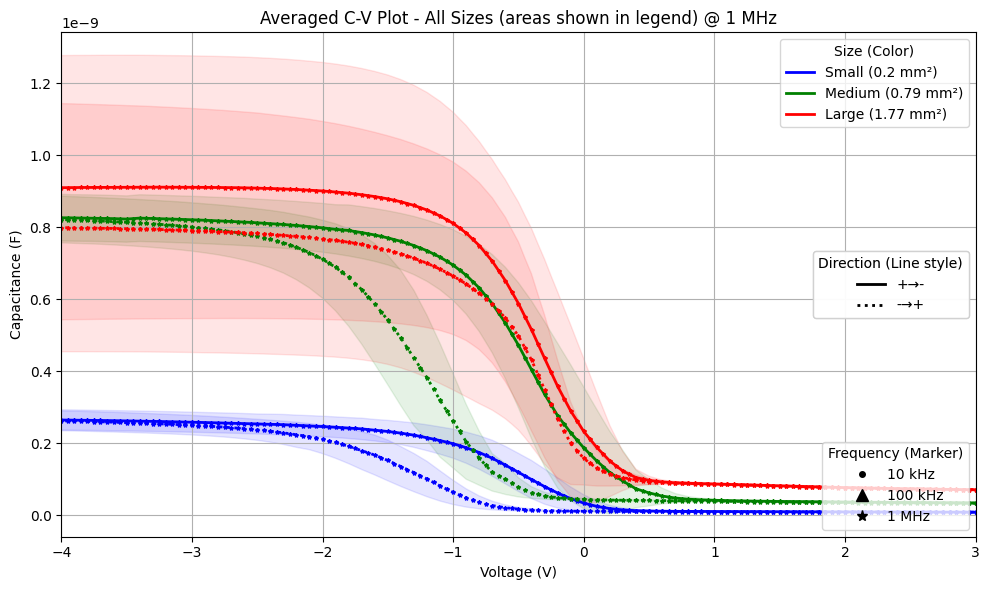
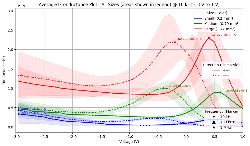
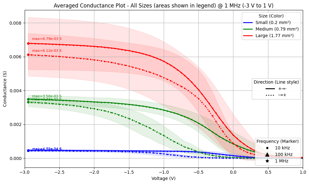
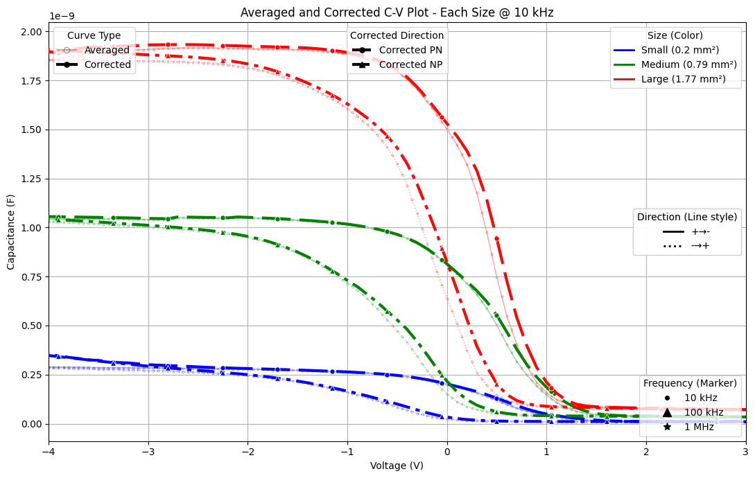
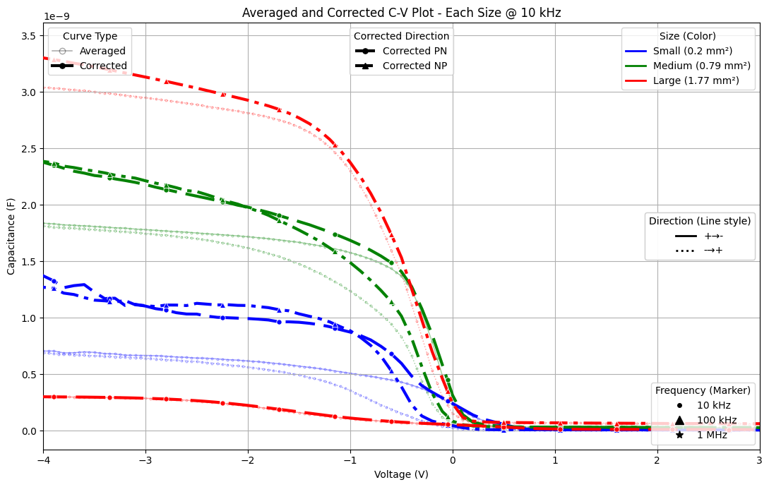
The plot below demonstrates the measurement technique applied to MOSCaps fabricated on the 5-10ohm p type wafers. Both C and 1/C^2 axes are plotted to clarify what region of the CV plot was used for calculating the donor/acceptor concentrations.
{% file src="/files/tSncAX6ndQToVy4iOh59" %}
[Tektronix CV Applications Guide](https://www.tek.com/en/documents/application-note/c-v-testing-semiconductor-components-and-devices-applications-guide)
It is important to note, that acceptor/donor concentration is what's calculated, not the actual concentration of Phosphorus or Boron. They can be different, since the P directly counteracts the underlying Boron doping, and if the P does not end up on a substitutional site it may not act as a donor. This may explain some discrepancy between the modeled and experimentally measured values for donor concentration seen below.
The plot below demonstrates the measurement technique applied to MOSCaps fabricated on the 5-10ohm p type wafers. Both C and 1/C^2 axes are plotted to clarify what region of the CV plot was used for calculating the donor/acceptor concentrations.
{% file src="/files/tSncAX6ndQToVy4iOh59" %}
 The plot below shows the doping concentration calculation for n type 1-10 ohm wafer with no diffusion as well as one with 5 min 800C predep + 1100C 1 hour drive in (on n type wafer). The choice of testing the diffusion conditions on an n type wafers was purposeful. If p type wafers were used, the n well would also create a conjunction in series with the MOSCap which can distort the CV measurement, so n type wafers were used as the starting substrate.
 | Sample | Expected concentration (N) | Measured concentration (N) from MOSCap CV |
| ---------------------------------------------------------------- | ------------------------------------------------------------------------------ | ----------------------------------------- |
| p type 5-10 ohm wafer | 2e15 /cm^3 based on [BYU calculator](https://cleanroom.byu.edu/resistivitycal) | 1.71e15 /cm^3 (acceptors) |
| n type 1-10 ohm wafer | 1e15 /cm^3 based on [BYU calculator](https://cleanroom.byu.edu/resistivitycal) | 1.08e15 /cm^3 (donors) |
| 800C 5min predep + 1100C 1hr drive in (on n type 1-10 ohm wafer) | 9.5e17/cm^3 based on diffusion model above | 2.05e16 /cm^3 (donors) |
The measurement shows that the 800c 5 min predep with 1100C 1hr drive in yields 2.05e16 /cm^3 donor concentration, which should yield a Vt of \~1.2V based on the Vt vs N calculations.
Next step is tuning the PMOS S/D p type regions to remain isolated and within the n well.
## Appendix
#### 9:9, 3hr, Standard RCA Clean
| Sample | Expected concentration (N) | Measured concentration (N) from MOSCap CV |
| ---------------------------------------------------------------- | ------------------------------------------------------------------------------ | ----------------------------------------- |
| p type 5-10 ohm wafer | 2e15 /cm^3 based on [BYU calculator](https://cleanroom.byu.edu/resistivitycal) | 1.71e15 /cm^3 (acceptors) |
| n type 1-10 ohm wafer | 1e15 /cm^3 based on [BYU calculator](https://cleanroom.byu.edu/resistivitycal) | 1.08e15 /cm^3 (donors) |
| 800C 5min predep + 1100C 1hr drive in (on n type 1-10 ohm wafer) | 9.5e17/cm^3 based on diffusion model above | 2.05e16 /cm^3 (donors) |
The measurement shows that the 800c 5 min predep with 1100C 1hr drive in yields 2.05e16 /cm^3 donor concentration, which should yield a Vt of \~1.2V based on the Vt vs N calculations.
Next step is tuning the PMOS S/D p type regions to remain isolated and within the n well.
## Appendix
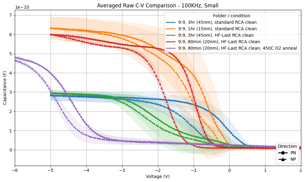
#### 9:9, 3hr, Standard RCA Clean