Accurate Graph of Cost to Build Hacker Fab vs. Semester (More DIY Designs)
Link to General Lab Equipment BOM
BOM of each machine is included in separate build documents.
Contribution Guidlines
The goal function of the Hacker Fab is to never debug the same thing twice.
We operate under different constraints from the semiconductor fab industry. This allows us to curb a lot of complexity.
Goals:
Low cost
Create the simplest designs possible
Increase reliability
Reduce manufacturing complexity
Minimal danger
Small size
Minimize required infrastructure
No cleanroom needed
Highly sourcable materials
Things to include in documentation:
BOM
Build instructions
Required tooling for build
Required infrastructure
On Improvement
Central to the Hacker Fab is fast turnaround hardware development - it’s in the name. This means extremely fast hardware prototyping, and with that comes the need for iteration. The careful design constraints placed on all projects and focus on documentation enables someone else to iterate on anything developed in the Hacker Fab. Improvement to a V1, V2, Vn of a design means
Directly improving upon a tool’s functionality
Precision
Reliability
But there are other equally important ways to improve a design. Every tool version should try to be:
Easier to manufacture than the last
Reduce number of tools required to manufacture
Reduce # of vendors, lead time, BOM length
Part Sourcing
Strategies for sourcing parts effectively, and a constantly updated list of part suppliers
Tool specs as close to first principles as possible
Every tool spec should have a standardized test for others to verify performance
Explain working principles to the detail of variables we can control (no more, no less). Referenced sources.
More “closed-loop” than the last
In-situ sensors
Calibration software should be more generalizable (“now you can use any camera…any piezo with draw distance in range X to Y…”)
The Way we Source Parts
Use ChatGPT to Source Parts for You
With Bing feature, you ask "source ___ for me" and add other details:
"prioritize parts with low lead times"
"inexpensive" or "hobby level"
"i liked this one you found, find me more of those"
Find the Part on Amazon
Nothing is better than prime shipping
If you found a part on a manufacturer's website, look up that exact part
If you cannot find it, try searching for the manufacturer's amazon page
They normally have one
Avoid "Contact us for a Quote" at all times
We try our best to not support companies that do this. If you ever start a company in the future, put a "buy now" button please.
Long lead times, wasted time talking to someone, different prices if you are a university, company, individual, they try to package you in with expensive software, etc.
If you don't know which part to buy, use ChatGPT
"what else are these parts called? anything else I could use instead"
"I am trying to find a part that does X, Y, and Z, but I don't know what its called"
"I am trying to attach ___ to ____, what can i use?"
As a last resort, you can contact manufacturers
Some teams, such as Thorlabs, Kurt Lesker, Filmtronics, are very knowledgable and can help bridge the gap of understanding. You can describe to them your situation, send them links of the parts you were considering, and ask them for their advice. Do this sooner rather than later - they take multiple days to respond.
Etching
Nothing yet!
Tube Furnace
All articles in this section are written by Nathaniel Jordan
Tube furnaces are often used in the heat processing steps of refining silicon for use in microchips and transistors due to their ability to safely reach temperatures of over 1000 oC using less power than that of typical ovens. The tube shape of the furnace allows for the introduction of steam and other diffusing substances using the process of heating, allowing for rapid oxidation or diffusion of dopants onto polished silicon. However, efficient tube furnaces often come with four figure plus price tags attached, and are often lab grade machines to withstand the repeated subjection to high temperatures. Despite this, tube furnaces are not particularly complex in construction, if the user's goal is simply to use the machine to safely achieve the high temperatures needed to create semiconductors. Although a homemade furnace would likely not be up to standard with an industrial tube furnace, the absence of luxuries such as ease of diffusion, control system regulation of temperature, and minimizing external factors means that, in an educational environment, forging semiconductors can be simplified to a high school level of understanding. Additionally, there is more freedom in the process as a result, allowing for instructors to slow down or explain certain processes to a greater degree, and for hobbyists to have more control over certain aspects in the process.
Example Student
My name is Joshna and I will be working on the SMU and Database this semester
Weekly Update #1
I did some preliminary research, you can find the task for this in github project tracker here: xxx I drew some schematics for the Database, which can be found in the master doc here: xxx. I am facing the challenge of IV curves appearing to be limited by power so I am reaching out on the Diligent forum. My plans for next week are to do these GitHub project tracker tasks:
Weekly Update #2
I was able to complete all the Github project tracker tasks I set out to do last week as well as talk to the lab automation team to figure out what they need from us on the database.
Yang Bai
Update 0
Filling in the Gaps - Background Resources
Semiconductor research has been around for decades, which means there are many people who can explain concepts better than we can. This is a collection of our favorite resources we've found.
This stuff is regularly communicated as complex , and requires the permission of to work on it. We are starting from 1960’s level complexity and working our way up to modern complexity.
(30 min)
Extremely well told story of the man who figured out how to manufacture blue LEDs
We are not the first people to claim that innovation in the semiconductor industry requires intimate knowledge of the fabrication tools
(∞)
A fantastic tool being developed by friends at MIT. Overview of many processes, with each being a linear recipe
Make an account, and go to “fabubase” in menu
Check out our Hacker fab process, as well as others
Below: ideal transistor IV curve vs. our first curves.
These both exhibit transistor-like characteristics. Looking back at the Veritasium video about how the first computers were made with lightbulbs - a transistor really boils down to a repeatable switching action. When we look at our curve on the right, we see multiple issues:
The curves don’t go through the origin, they start with a voltage offset
This means that when we apply a voltage to the gate (open the valve to allow current through), current doesn’t run through the drain to the source until we apply ~3V to the drain/source connection.
The lines are all squiggly?
So we try to debug this by finding literature that debugged something similar, or often we simply design and run more experiments. Skim through pages 172-176 (bottom corner number, not pdf page number) of . Their transistors have very similar issues to ours. When you read this document, the answers are behind a huge layer of jargon and acronyms that make the barrier to entry for understanding extremely high.
In reality here is what it is saying:
Our source-drain is dominated by an aluminum metal-to-silicon instead of doping
Put simply, we just directly connected an electrical characteristic (IV curve) to a physical process parameter. We now have an exact experiment to try over the next week:
Less metal annealing
More Si02 etch before metal deposition (to ensure metal contacts Si instead of SiO2)
Right now it takes about 8 hours of work + waiting overnight to turn a blank wafer into one with NMOS transistors on it. Then we go to the probe station, test it, organize the data, look at the graphs, and think. That’s how long it takes to verify each new experiment. With each machine, script, or management tool we create, we push to significantly decrease this iteration cycle.
We've only made NMOS devices so far, but there are to be made. That means our process data corresponds to NMOS only, but most process steps can be generalized to any process if documented properly.
Each unique device can also use different materials entirely, which requires different machines.
What metal are we depositing?
What does the doping profile look like?
etc.
Deposition
Annealing
Oxidation Chart & Results
When introduced to steam inside the tube furnace, blank piece of silicon can be oxidized. The color of the oxidation varies on the time, heat, and amount of steam introduced, but the color tends to oscillate based on the thickness of oxidation. Below is a chart of samples comparing the thickness of oxidation to the wavelength of light the sample is observed under. The thickness increases with more time spent in the furnace. Samples were collected in one test run for consistency sake.
Source doc can be found at: https://docs.google.com/document/d/1FCWTG4O32Z9_obltcXkp06KeX1oHtoSjYk6xLp93loU/edit?tab=t.0#heading=h.qtlewtj99lm8
Read in google doc link above for now ^
To be transferred to gitbook
Matthew Choi's Updates
1st week: reviewed the hackerfab syllabus and got registered on gitbook
Week 5 Update
What was accomplished:
Finished designing the peristatic pump, and got the 27:1 gear motor attached to the mechanism
Researched syringe pump method as an alternative option in case the peristatic pump wouldn't work. Designed several diagrams, but before reaching CAD phase, found a lot of critical drawbacks that convinced me to use the peristatic pump instead(including linear actuators that require built in encoders)
Start working on PPT for the presentation on tuesday
Roadblocks:
3d printed parts for the pump(may be accurate, but should have initially been designed to account for clearance holes for drilling through)
Finding the right material for syringe pump(a glass syringe would be optimal to handle all the liquids required, but the larger models do not have built in syringe needles, so a glass syringe + recyclable needle with luer locks was thought out)
TO DOs:
Finalize PPT for tuesday
Help Advaith move the pump mechanisms into the overall assembly, as well as implementing other components(Im not sure how the spin coater is going to look like)
CMU Updates
As part of CMU's Hacker Fab Course 18469/18669, students will give updates on their project work every Sunday night.
7/3 - Furnace 5 kanthal wire double twisted fried, had to reattached ceramic wire
7/14 - Furnace 5 ceramic wires fried, first attempt after previous repair, was running for 3+ hours
Hot Plate SOP
Purpose
Soft baking photoresist and annealing spin on glass.
Spin on Glass Storage and Preparation
Long Term Storage
The SOG from Filmtronics found , has a shelf life of around 3 months when stored at room temperature. For this reason, the bulk SOG bottle must be kept in the fridge at around 32-40 F in order to extend its shelf life. Exposure to air and/or heat can cause some of the SOG vapors to harden. If this happens, flakes of SiO2 may form and contaminate the liquid solution.
Wafer Cleaving SOP
Purpose
We pre-dice wafers in order to:
NAND + Inverter Characterization
Fabrication and Testing of Enhancement Load NMOS Inverter Based on HackFab’s Standard Process Flow
Introduction
NOT gate or inverter outputs the opposite of its input as shown in Table 1 is a basic but crucial part of the digital logic circuit. An NMOS logic inverter normally consists of two parts, a resistive load connected between the supply voltage (VDD) and the output as the “pull up” part and a switching transistor as the “pull down” part. To save device area and fabrication cost, instead of using resistors for the load, an active load such as an enhancement load transistor is used in the design as shown in Figure 1 (left). Enhancement load means a transistor’s gate and the drain are both connected to the supply voltage and make the transistor always in the saturation region. However, this causes there will be a constant current going through the transistors even if it is not performing which makes NMOS logic technology have higher power consumption and eventually be replaced by CMOS technology.
CMOS Doping Process Development
Dope the channel, and source/drain regions for CMOS chips, via solid source surface diffusion, starting with 5-10 ohm p-type substrate.
Metrics
CMOS Region
Doping level
Doping Profile Details
Week 2 Updates
3d printing shenanigans + getting started
Before receiving updates on what I was supposed to work on this week, I helped Anirud re-CAD and 3d print several modified components of the Spin coater. The dimensions of the spin coater were increased in length by 45 mm, and the holes for buttons were more enclosed together due to wire entanglement concerns, and the buttons not being fully optimized for assembly. Along with that, the holes for motor attachment were slightly modified so that all four screw holes would accurately fit in the motor. The height of the vase was also slightly decreased to account for the addition of a top plate on the spin coater. All of these revisions ended up significantly increasing the efficiency of the spin coater's ability to hold silicon in place. The only major roadblock along the process was failing to recognize that the BAMBU 3d printer had different setting from the default BAMBU settings, as well as the PRUSA filament toppling over, resulting in some prints being scrapped.
I additionally began to conduct research on the pinch valve mechanism that I discussed with my fellow lab automation teammates, and began investigating the pros and cons of utilizing such a design in contrast to the original peristaltic pump. The pros include the fact that the basic mechanism for the pinch valve is a lot less complex, since it involves one or two motor simply twisting a screw to completely enclose water flow. The major downside is that a large majority of pinch valves attempt to "pinch" by enclosing both sides of the tube instead of only one.
Week 3 Updates
The great re-vamp
The lab automation team received an update this week that we basically had to re-vamp a large portion of the project, since the gantry was(apparently) no longer deemed necessary. Our goals were reset so that everyone on the team was set to work on the "NEW" lab automation plan, which was to combine the liquidation handling, the spin coater, and the thermal heating system.
For starters, me and the rest of the team took a look at an iteration of the three in one spin coater that was already on the internet(and made at an extremely cheap price) as well.
Of course, since this was an extremely low budget design, we realized that there were several improvements we could make. For starters, the liquid handling system is basically composed of a single syringe, as well as a better solvent catch bowl system to collect excess liquids. Along with that, a more efficient vacuum system would benefit the spin coater, since the current iteration does not suction the silicon hard enough to keep it in place consistently at higher rpm.
CMOS Source/Drain Metal Contact Optimization
Goals
Develop metal contact formation process (pre, during, and post deposition development) to reduce the contact resistance and Schottky behavior of of metal contacts on Source/Drain regions of PMOS and NMOS devices. Metal type in metal - Si contact is part of optimization.
Week 6 Update
What was accomplished:
Finished working on the PPT for Tuesday, and took major feedback on issues with peristaltic pump(including potential issues with air being pumped out instead of actual liquid)
Re-designed a spin coater to fit on to the overall automated assembly
Week 7 Update
Spring break also added
What was accomplished:
redesigned original spin coater design to suit Lab automation needs(by removing all mounting needed for LCD and buttons, and minimizing dimensions to fit the assembly)
designed the syringe liquid handling design CAD on onshape, as well as ordering components for them
Read about other spin coater + liquid handling setups, and how they managed to deal with liquid handling consistency issues(THEY USED SYRINGE NEEDLES SINCE THEY WILL PREVENT LIQUID FROM FLOWING DOWN WHILE AIR CAN SO ATTACHING IT TO THE SILICON WOULD SOLVE POTENTIAL ISSUES WITH NON-CHEMICALS)
Not sure if the current silicone tubing for the peristaltic pump is small enough to attach re-usable syringe needles
Need to debug peristaltic pump accuracy for accuracy regarding how consistent liquid handling is(we can do something like 3 trials for consistent 5 ml of liquid to debug)
TO DOs:
CAD a new control panel for the overall raspberry pi setup
Order components for SMALLER silicone tubing with luer locks(that can attach a syringe needle), as well as linear actuators and silicone/glass syringes, since they allow easier control of precise liquid handling control
The largest road block
as of now, is figuring out if there is an efficient pinch valve design capable of "pinching" the tube on both directions with one motor, while also being compact enough to fit with the rest of the lab automation components. Furthermore, the pinch valve is not suited for high temperature purposes, and I am not completely sure what temperatures the liquids will be operating in.
For next week, I plan on CADing two or three different iterations of the pinch valve, depending on if I determine that pinching the tube on both ends is possible with one motor. If possible, I will attempt to use FEA to determine if the liquid flow through the valve is minimized and compare the designs and check which one offers the least liquid flow.
Furnace 6 ceramic wires fried, first attempt, ran for 20+ minutes
Thermocouple side
Entry Side
Ceramic coating on both furnaces was disintegrating where wires had contact
Ceramic beads seem a little burnt but otherwise intact, Furnace 5 and 6 each had one ceramic wire still in contact with kanthal, being held together with bead despite being fried → possible only the thermocouple wire side was completely fried through, however it’s clear that both wires are under severe heat stress during operation
7/15 - Discovered kanthal wire coil on furnace 6 had been burned and rusted through
To combat this, next tube was made with as few kinks in wiring as possible, and the kanthal wire is used as the connector to the motor control as opposed to ceramic coated copper
8/25 - Since switching wiring to full kanthal and using one solid piece of wire, shorts have been discovered in the machines after repeated use. Found out the cause was due to the weave casing of wiring was being shredded through
9/8 - Incorporating the PID controller with a lack of motor control results in too much current being drawn and the kanthal wires becoming so hot they burn through the insulation weave
9/9 - Incorporated motor control into PID wiring to control current, but creates a problem where current is not being drawn unless an additional element, such as a lightbulb, is incorporated to trick the system into powering on
Thermocouple side
Entry Side
Troubleshooting and Best Practices
Mark a single location on hot plate to place chip throughout every experiment to minimize temperature variation
Very inconsistent heating zones on most hot plates. These are not manufactured for 1cm^2 chip heating, original purpose is for heating of large beakers and liquids.
A 400C hotplate is barely warm on the edges
Procedure
Heating
Plug in the hot plate, it should beep, light up the screen, then go dark.
Switch the hot plate on, it should light up and display both current temperature, and a pending set temperature.
Turn the knob until the desired set temperature is present, hold the knob down until it beeps to set the desired temperature.
A small green circle should appear at the set temperature
The screen should alternate between set temperature and current temperature, ensuring that the current temperature is increasing.
Increasing Set Temperature While Operating
Hold the knob down until the set temperature is canceled.
The small green circle should turn off.
Turn the knob to your new desired temperature, hold the knob down until it beeps to set the desired temperature.
A small green circle should appear at the set temperature
The screen should alternate between set temperature and current temperature, ensuring that the current temperature is increasing.
Shut Down
Hold the knob down until the set temperature is canceled.
The small green circle should turn off.
Switch the hot plate off.
Unplug the hotplate.
Store bulk SOG in fridge (32-40F)
Shelf life of bulk is 3 months at room temperature
Short term Storage/ preparing small amounts for use
Replace Every 2 weeks
Use a small plastic container (insert pic) to store a small amount ( < 10 ml) of SOG. Label the container as “700B” (undoped) or “P504” (dopant) and label the date that it was transferred from the bulk supply.
Store this bottle of SOG at room temperature under the fume hood where SOG spin coating and annealing is performed.
Allow the SOG to come to room temperature prior to use
Filmtroonics recommends to allow the SOG to come to room temperature for 24 hours but this can be shortened to just a few hours if < 5 ml of SOG is in the bottle
Inspecting SOG bottle prior to use
Ensure the SOG has come to room temperature
Check the bottle’s date. If the SOG was transferred from the bulk supply more than a week prior, it is likely necessary to prepare a new bottle of SOG
Regardless of the date on the bottle, open the bottle to check if any crust has formed near the top of the bottle. If there is any visible crust from hardened SOG, it is necessary to prepare a new bottle of SOG
The crust formed can get into the liquid SOG applied before spin coating and ruin the SOG coating
Example of crusted SOG from a bottle that has been used for too long
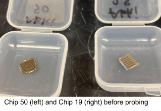
Open this central chip count sheet, claim the next available chip number, open the blank chip view sheet for that specific chip number and record all subsequent process data into it.
If the surface has some give, it will act as a spring when pressure is applied from the scribe
At an oblique angle, place the scribe tip at the edge of the flat side of the wafer
Flat edge marks crystal orientation, cleaving should be easier along certain crystallographic directions.
Push down, don't think too hard, cleave.
It may also help to press down and drag the scribe tip 1 mm outwards to the edge of the wafer.
Don’t move chip around with the diamond scribe to avoid scratches
Use to move once a cut is made
When it comes to major roadblocks, several new variables came into mind once we decided to merge all the components of lab automation into one. The biggest one for sure as of now, is the fact that we may have to pursue a different filament or material for the base of the spin coater due to there being a solid chance of it not being able to withstand the heat. The original spin coater was also not stationary enough(due to how light it was), so utilizing aluminum as the base instead was a suggestion that came to mind. Other roadblocks include, as mentioned, improving the vacuum system of the spin coater, minimizing motors(since the less moving parts, the easier time we will have), and attaching an updated liquid handling system that can alternate between different chemicals(since we have to differentiate which liquids are which within the tube)
For next week, I plan on initially CADing the base design of the spin coater(while taking into account the liquid handling + thermal heating) , and attempting to help Adwoa move her Fusion360 file of the perstaltic pump to onshape(while maintaining her sketches).
Model, frame, electrical connections, and action process of the budget multipurpose spincoater
Wrote down the hackerfab midsemester documentation
Roadblocks/issues:
Finding the right syringe for liquid handling, since the main issue was finding a syringe with the right specifications. We needed our syringe to be made out of PTFE or glass, but a majority of the ones we found were made of polyethylene, which would eventually wear out due to acetone and IPA.
The measurements for the nozzle of the syringe that we ordered was flawed(2mm is not equivalent to 0.4 inches), so we had to take into account the chance that the nozzle isn't the same measurement as advertised
The nozzle of the syringe was also not meant for locking syringes(but were still ordered in case we would switch back to plastic syringes), so we would have to potentially find a way to attach a needle onto the tubing from the syringe
TO DOs:
Debug the lead screw stepper motor we have to calibrate the amount of liquid would needed to coat/clean a chip
Hacker Fab Documentation
the first open-source semiconductor fab.
intro.
Our Goals:
Make a DIY version of every nanofabrication tool
Get there with collaborative open source hardware
Nanofabrication labs are expensive and inaccessible. Even STEM students at "prestigious institutions" have limited - if any - access to nanofabrication tools. Chips run our world. Everyone deserves access to the tools that make them. To ensure this level of access; cheap, open source, and easily replicable nanofabrication tools are needed. Labs that make and utilize these open source tools need to appear world wide. Hacker Fab is the open source fab project making this happen. As of March 2026, seven Hacker Fabs have been established, while others are underway. Multiple critical open source fab tools have been built, documented, and duplicated. Countless devices have been demonstrated with these tools, with documented process development.
Hacker Fab has is made possible by a delocalized community of contributors. Hacker Fab can only grow to its full potential by gaining more contributors. Anyone can contribute, see the next section to learn how.
contributing to the hacker fab.
We communicate over.
You don't need to build an entire fab to contribute, .
Read the .
You don't need prior nanofabrication experience to create meaningful contributions.
How to add your work to the gitbook:
Hit the button that says "contribute"
Find the appropriate spot in the gitbook to add your work. For new projects this may be a new page, for modifications to existing work this could be an edit or amendment to existing pages. Fill in your contributed content.
Note, if you download your working document(s) (google docs for example) as zipped .html files, you can them import them directly to a new gitbook page. This will maintain most of the content and formatting from your working document(s).
this website.
This page is a home for all shared documentation. There are enough resources here to turn an empty room into one that fabricates simple IC's in a matter of months.
Many pages are works-in-progress. It is natural for individual contributors' work-in-progress notes to exist on google drive, notion, etc. Links to these exist at the top of each page, however these notes move to Gitbook as soon as possible.
Any contributor can submit change requests with a free Gitbook account. All of this is on Github, but formatted nicely here on Gitbook. You can contribute directly through Github as well.
For the most up-to-date status on everything, join the.
fab toolkit.
verification / metrology tools.
chemicals.
background and licensing.
The Hacker Fab was inspired by .
The Hacker Fab was started by Elio Bourcart, Alexander Hakim, and Sam Zeloof at Carnegie Mellon University (Thank you to CMU ECE dept, who's support catalyzed the project).
The first is and currently managed by Matthew Moneck, Tathagata Srimani, and Jay Kunselman.
By default, all contributions use the following license stack, but may carry an additional NOTICE file depending on the origin of the contribution.
Hardware: CERN-OHL-W
For example, if you release HDL files under CERN-OHL-W and then somebody uses those files in their FPGA, when they distribute the bitstream (either putting it online or shipping a product with it) they do not to make the rest of the HDL design available under CERN-OHL-W as well.
Software: MPL v2.0
The MPL’s “file-level” copyleft is designed to encourage contributors to share modifications they make to your code, while still allowing them to combine your code with code under other licenses (open or proprietary) with minimal restrictions.
Documentation: CC BY-SA 4.0
This license enables reusers to distribute, remix, adapt, and build upon the material in any medium or format, so long as attribution is given to the creator. The license allows for commercial use. If you remix, adapt, or build upon the material, you must license the modified material under identical terms.
Patterning Tasks - Spring 2025
This page documents the current work being done on patterning systems and the goals of that work. If you want to start a new project or research related to patterning, add it here so we can keep track of what's being done!
Task
Metrics
Timeline
Task Lead
Backlash Improvements
<2µm backlash
Before February
Carson Swoveland (@_salix)
Absolute Positioning
<5µm accuracy+precision
Backlash Improvements
The current design for stepper v2 involves having the micrometer-motor couplers slide along the shaft of the motor. This leads to wear in the 3D print and prevents the use of a rigid connection, leading to the coupler eventually becoming loose. This can cause ~30º of backlash in the rotation, which corresponds to about 15 microns.
Mounting the motors on the stage that they move, rather than on a (relatively) fixed stage allows for using a rigid coupling without significant modification to other parts of the design. These fixes should be applicable to any fab with an existing v2 stage. This is a major enabler for .
This may require redesigning the stage to be mounted upright, or the stage to be turned sideways.
The WIP CAD files are available on and more information can be found .
Absolute Positioning
In order to enable many features like automated or computer-assisted patterning, it must be possible to consistently refer to positions on a die. This requires being able to determine the absolute position of the stage.
There has been some experimentation with using inductive sensors for determining the stage position, though calibrating and mounting the sensors is difficult. The accuracy for a properly calibrated and mounted sensor may be sufficient, though. (TODO: Link inductive sensor notes once those get merged)
Currently, a design using simple limit switches is being developed (though blocked on ).
Cost Reductions
The current optics system is not physically capable of handling the projector's resolution, i.e. some amount of detail is wasted in the optics system. This means that we can use a lower resolution (read: cheaper) projector.
There are two main items that we are looking at replacing to reduce our cost. The first is the projector itself, as we are using an expensive 4K projector that does not appear to yield much benefit in patterning resolution. We are considering going from the ($999) to the ($299).
The second item that we are looking at is our camera. We are currently using a high-resolution ($700) which, again, is excessive for our application. We believe that we can find a similar C-mount camera for less than $200.
Lastly, there are other components in the optics system itself that we believe can be modified/replaced to further reduce the cost. The ThorLabs components cost at least $700, but many of those parts such as tubes and flanges could be replaced by 3D-printed parts. We will have to test to see if heat generated by the stepper becomes an issue, but this would provide a significant reduction in cost.
Altogether, we believe that we can bring the cost of the stepper below $2000 - perhaps even $1500.
Vacuum Spin Coater SOP
DIY Vacuum Spin Coater Hooked up to Rotary Vane Pump
Purpose
To apply a thin layer of wet chemicals to the surface of the chip, with sub-micron control.
Troubleshooting and Best Practices
Spin Coater is Stuck, the chuck tries to move but it stays in place
Remove the outer plastic vase that holds the residual photoresist and chemicals
Wet a cleanroom wipe with acetone and wipe the outside of the chuck and the inside of the plastic vase clean
Procedure
Plug in the Spin coater and the vacuum pump (if either is not able to power on try hitting “reset” on the outlet)
Use the arrows on the touch screen to set the spin time and rpm
Use tweezers to place wafer onto the o-ring so that the chip completely covers the o-ring and will seal onto it
Side Notes
If you hear the spin coater constantly beeping, this is normal. It does this because we are using a drone motor ESC, so it is programmed to make a noise after being at rest for a few minutes. It’s trying to help you find it 🙂
Feel free to turn it off using the switch in the front so the noise goes away.
Photoresist Strip SOP
Example of Photoresist on Surface of Chip
Photoresist Removed post-strip
Parameters
Total Time
1 minute
Acetone Spray Time
Purpose
Stripping removes all photoresist from a chip. This is typically done after an etch step is completed, though it can also be used to remove resist before etching if you need to redo patterning.
Tools
Fume Hood with Sink
N2 gun
Materials
Chip with photoresist
Acetone
Isopropanol
Troubleshooting and Best Practices
Chip flying out of tweezers during nitrogen blow drying
Lie the chip flat on a cleanroom wipe surface while still holding it with the tweezers.
Only apply nitrogen normal to the surface of the chip, so it presses against the cleanroom wipe instead of lifting it up.
Procedure
Stripping
Spray the entire chip with acetone
Rinse with IPA
IPA must always be used after acetone to remove any acetone residue
Safety
Be sure to spray the chip over a sink. Do not use near source of high heat.
Dry Oxide Growth SOP
SOP for dry oxide growth of 10nm SiO2
Silicon before and after oxidation
Parameters
Temperature
1100°C
Total Time
30 min (subject to change)
Purpose
The oxidation growth of the silicon layer creates a layer of insulation to prevent direct flow from the conducting MOSFET layer to the metal gate.
Tube Furnace () with fused silica tube
Fused silica rod
Fused silica microscope slide
Tools
Tube Furnace () with fused silica tube
Fused silica rod
Fused silica microscope slide
Materials
Pure silicon chip (not pre-deposited)
Procedure
Pre-heating the Furnace
Turn on the furnace.
Press and hold “set/ent” for three seconds until “mode res” is showing. Press the up arrow twice until mode “LCL” is selected. Press “enter” once. Now the furnace will hold the temperature shown. Use the arrow keys to adjust and press “enter” once to set the setpoint.
Wait ~15 min for the furnace to come to temperature.
Inserting chips
Put the fused silica microscope slide in the entrance of the tube. Do not use a regular borosilicate microscope slide, or it will melt inside the tube. The edge of a fused silica slide is pure white, while borosilicate is a little bit green.
A chip permanently fused to the tube furnace walls when improper slide was used 🔥
Place your chips on the slide.
Use the glass rod to push the slide into the center of the tube, being careful to not scratch the inside of the tube too much. Start the timer.
Place the rod on top of the tube furnace (it will be hot).
Removing chips
Use the glass rod to push the slide to the other end of the tube.
Push the slide all the way to the end until it is reachable.
Put the rod on top of the tube furnace (it will be hot).
Safety
The furnace is obviously very hot. Keep away from any hot parts of the furnace. The rod will heat up in the few seconds that it is inside the tube, so when removing it, only hold it by the end.
The rod and tube also channel heat out of their ends via internal reflection of radiation.
Sputtering Gate Oxides + Metal Gate Contacts
Motivation:
A metal oxide semiconductor field effect transistor (MOSFET) is essentially made up of two opposing PN junctions and a metal oxide semiconductor capacitor (MOSCap). The current Hacker Fab NMOS process begins with a wafer which already has 20 nm of SiO2 on the surface of the Si, and 500 nm of polysilicon deposited on top of the SiO2. In the final MOSFet device, the SiO2 acts as the oxide and the polySi acts as the “metal” in the MOSCap present within the NMOSFET. This process flow prevents the simultaneous fabrication of PMOSFETs, which is necessary to make CMOS devices. To make CMOS devices, we need to begin with a bare Si wafer, and make the MOSFets “oxide”/dielectric layer ourselves Due to this, and other concerns with the NMOS process flow, Hacker Fab needs to develop the capability to grow or deposit dielectric thin films to act as the oxide. However, the oxide is the thinnest film in the device, and the film most sensitive to impurities. For this reason, the process to deposit gate oxides is the most likely to have quality issues.
Based on this need, and surveying our options for making our own gate oxide, we began building an RF sputtering chamber in the F24 semester (@ CMU). RF sputtering has the capability to deposit thin films of dielectric and conducting materials.
Goals
Deposit 40-50nm thick Al2O3 layers to use a gate dielectric in CMOS process
Deposit 100 nm thick Al2O3 layers to make electrical contact to the gate dielectric, and protect the sensitive gate dielectric. This is to be done in the same process step as the Al2O3 deposition.
Metrics
Al2O3 Property
The metrics defined above are dependent on other metrics, such as stoichiometry, which is effected by processing parameters like sputtering power and O2 flow rate etc.
Al Metrics
Working Folder in Google Drive:
March 2026 Update
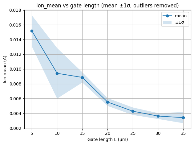
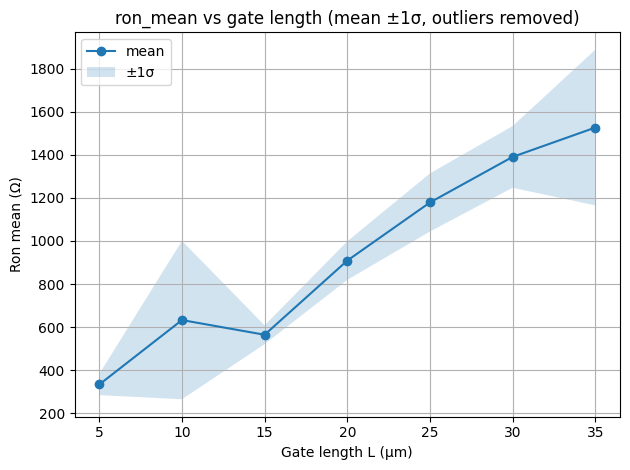
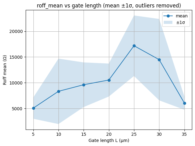
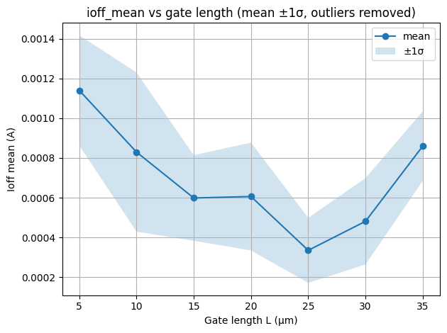
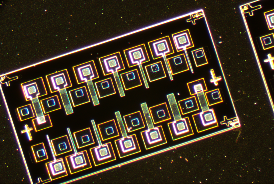
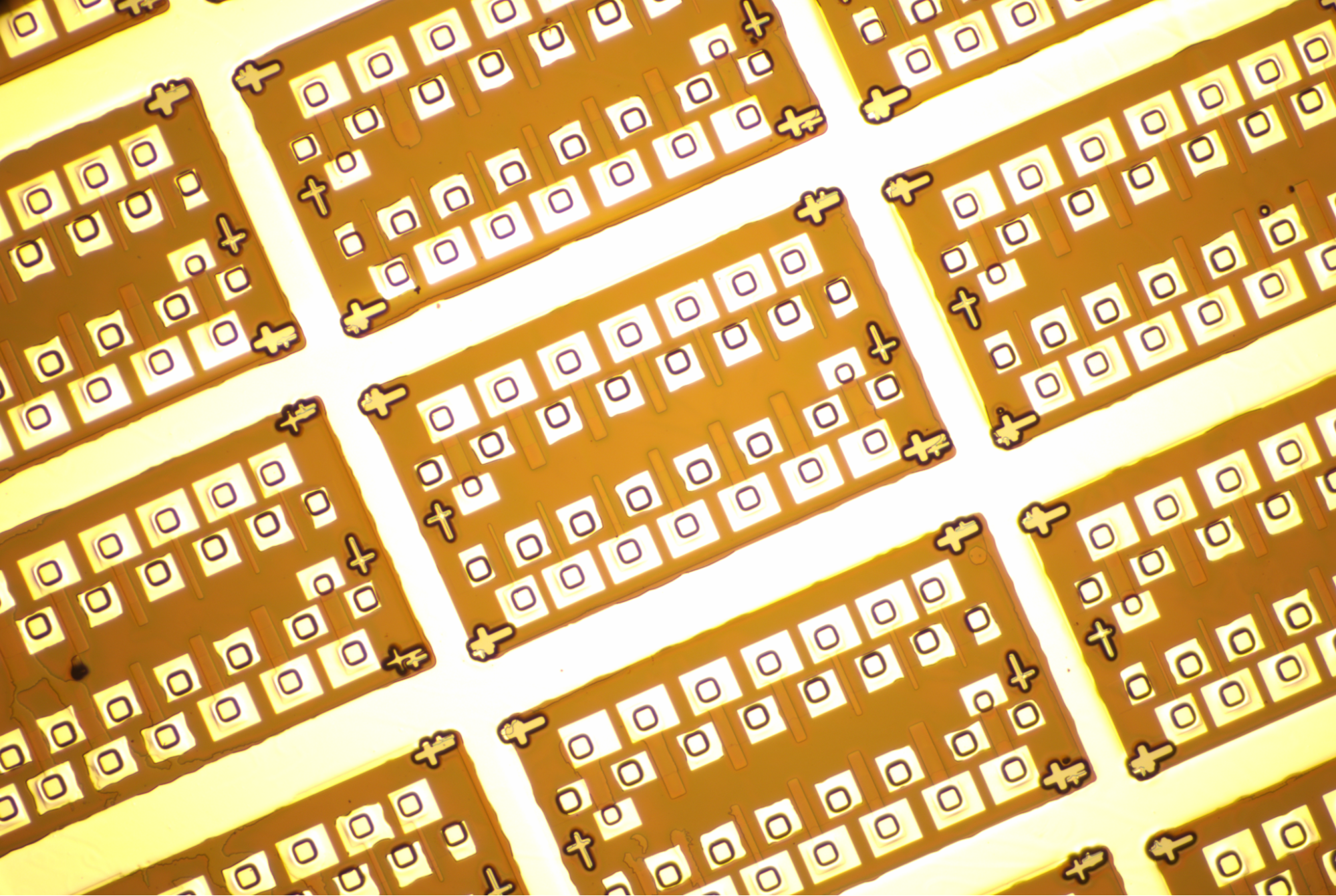
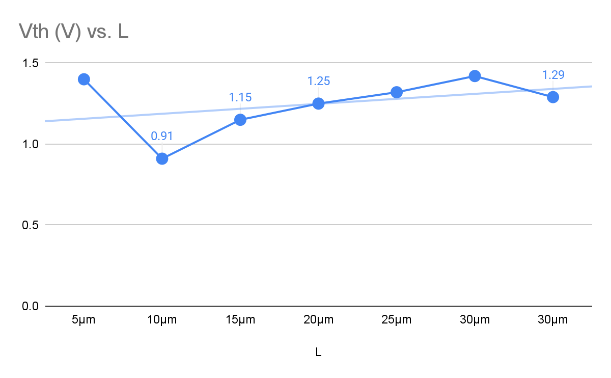
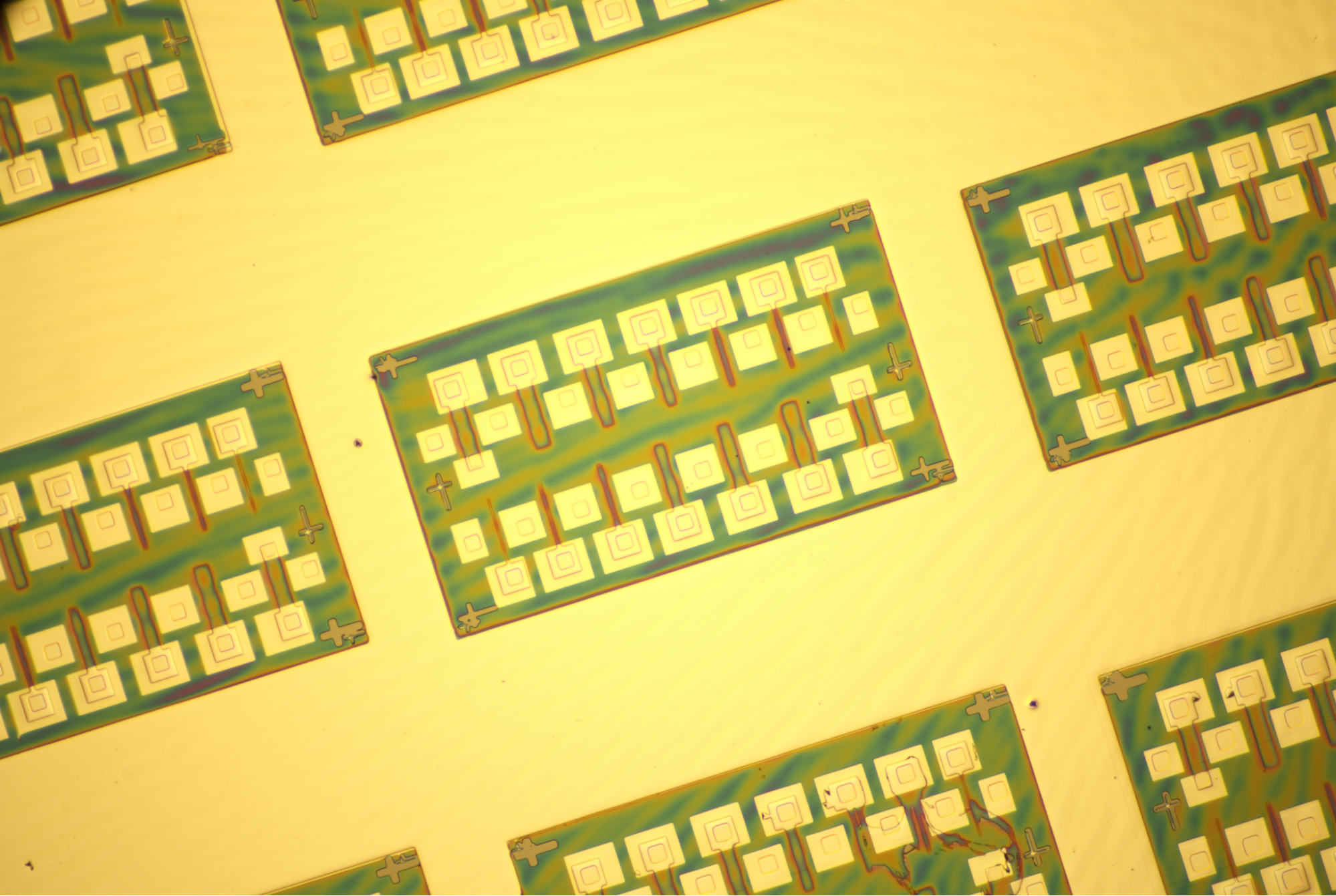
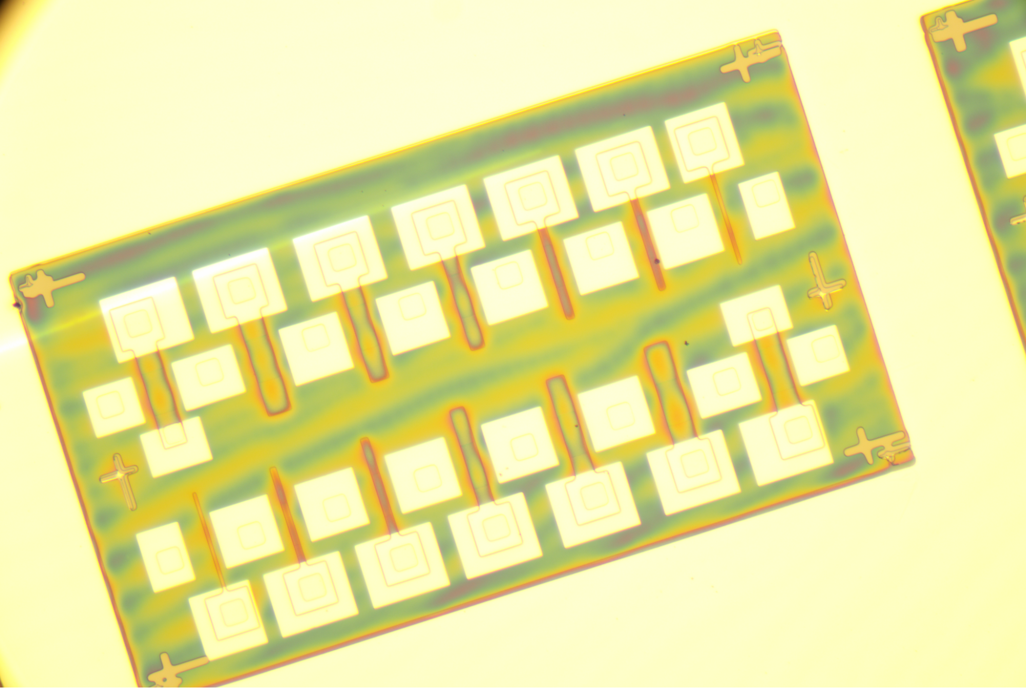
A team of 8 students (CMU Fab) Joined Hacker Fab in January 2026, learned the NMOS process, fabed over 1500 NMOSFETs and characterized them. Their results are documented in the sub pages below.
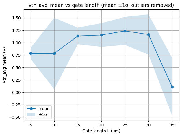
Overview:
952 Transistors per Chip
94% Yield
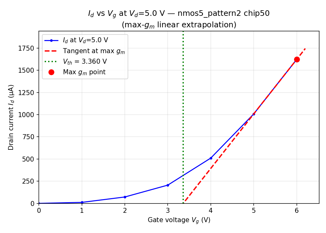
1.26V Threshold Voltage
5 um gate length
Tube Furnace 4: Aphex
Goals and operating parameters
The minimum goal of the Tabasco iteration of the tube furnace was to reach 1000 degrees C with no more than 1000 Watts of power. The ideal goal for Aphex would be to reach this temperature with around 500 Watts of power. Maintaining this temperature for long periods of oxidation is also important.
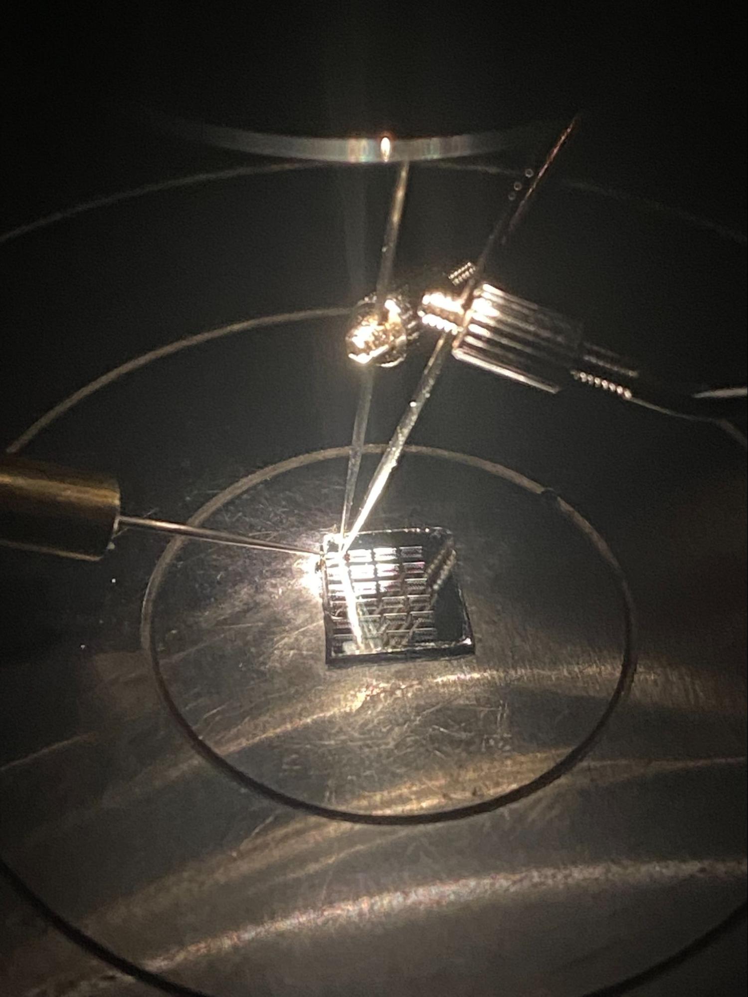
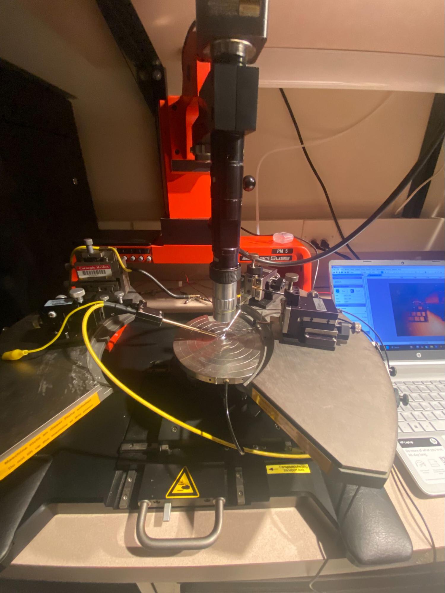
Probe Station SOP - V2
Version 2 of the probe station using analog discovery 3s
Purpose
After fabrication, the chip must be tested to demonstrate the functionality of the design. Additionally, variations and errors in fabrication may result in differences in device characteristics which are useful to document when these variations cause the device to fail.
To enable precisely controlled experiments on microscopic chips, we currently use a probe station to contact the device using sharp probes which supply and measure voltages for calculation of various device characteristics such as I-V curves, which are explained in this SOP.
November 2023 Update
Mask Generation and DRC
Source doc can be found at: https://docs.google.com/document/d/1ZS5bjdoCn44r_l2MRa-WB74HD4ZpJ85C6W1FY36Ok1k/edit?tab=t.0
Our Maskless Photolithography Stepper uses a DLP projector to create a pattern.
To accelerate the mask generation process for the needs of massive iterations in test patterns/ device dimensions for process development purposes, and achieve cross-tile alignment in the tiling technique. We explored methods, from existing EDA tools (KLayout) to developing programs using open source packages (PHIDL), to improve mask designing tools to be scalable, optimized, and automated.
Additionally, the masks created may not create components with the expected behavior. Design Rule Checking (DRC) is a crucial step when laying out circuits, and ensures the expected behavior of circuits by checking the distance, area, length, etc. of different blocks of material in different layers. For example, having metal blocks with different potentials too close to each other can lead to large parasitics, and having n-well taps too close to each other can result in them being combined.
Dry with nitrogen gun until the surface is entirely dry
This requires you to blow dry the back of the chip as well. Surface tension tends to pull the liquid towards the back
20 seconds
Isopropyl Alcohol Rinse Time
10 seconds
Nitrogen Blow Dry Time
10 seconds
If the furnace stops and holds at a lower temperature than your setpoint, the high temperature alarm may be too low. Read the instructions on page 6-7 to fix this.
Wait a few minutes for the slide to cool down.
Use metal tweezers to take the slide out. Don't use the orange ones because they don't close all the way.
Put the slide on a heat resistant surface and wait 5 minutes before handling the chip.
If the problem persists, run the spin coater without the plastic vase or any chip present, then press the acetone covered wipe against the chuck as it is spinning to get a thorough clean
Also attempt to center the chip on the o-ring as best you can. This will minimize the chances of it flying off.
Use a pipette to apply liquid on top of the wafer while it is seated in the spin coater. You only need a couple drops in the pipette, don't suck up extra.
Close the HMDS/photoresist/SOG lid.
Close the spin coater lid
SWITCH ON THE VACUUM PUMP!
Press “begin”
This will begin a pre spin at 600 rpm
Press “coat”
When the spin time has been reached, the coater will automatically ramp down to rest
Open the lid and remove the wafer with tweezers
Major components
The tube of the furnace is a 2 inch diameter quartz glass tube, with a center covered in refractory cement, and approximately 20 loops of double twisted 24g kanthal wire wrapped over the cement portion. This is wrapped in several layers of ceramic wool insulation, and then covered with sheet metal. The sheet metal is held together with shelf brackets and a handle. On the back of the tube is an attached thermocouple for temperature measurement. Other parts of the setup include a programmable circuit breaker to protect the local circuit from overloading, a motor control to control the voltage/current flowing into the furnace, and a voltmeter attached to the thermocouple for temperature readings.
24g, 20’+, wrapped into 20 loops around glass tube
Ceramic Wool
1” thick, cut to wrap once around the tube and to wrap around refractory bricks 5” x 5” x 1” refractory bricks
Thermocouple
8” long, mount has less than 2” diameter
Refractory Bricks
5” x 5” x 1” each, 2” hole cut through middle for glass tube, approximately 8 used and held together by refractory cement
Construction
1. Coat mid section of glass tube in refractory cement, score lines to allow for shrinkage during curing, let cure for several hours
2. Measure kanthal wire using the desired number of loops around the tube, with some extra length, then double the total length. Fold in half and twist the entire wire tightly using a power drill and tension. Carefully wrap wire around the cemented area of the tube, holding firmly. Hold with rubber bands and cement on top, let cure.
3. Wrap tube with wire in ceramic wool. Extend kanthal wiring to fit where the hole sites in the casing would be. Use ceramic beads to prevent contact between wiring and the casing. Connect ceramic wiring to the extra kanthal wiring.
4. Bend sheet metal into a box, drill hole to fit tube through as it sticks through insulation. Place the tube through sheet metal box. Drill holes for wires, add more ceramic beads to prevent contact if necessary. Pull the wires through the holes and fit the tube with insulation through the case.
5. Bracket the edges of the box, leaving extra bracket to allow the furnace to stand up. Fix in thermocouple.
Testing and performance
Failed 2x due to oxidation of ceramic wires while heating, 2nd attempt lasted long enough for several hours of oxidation and 3rd attempt lasted for entire process
Can maintain heat for long periods
Despite this, doesn’t hit power goal of 500 W for 1000 degrees C (~ 1000W), although closer than then previous iteration
Very light design compared to previous model
Things to improve on
Can be more efficient in trapping heat and power usage
Thermocouple could be mounted better
Very hard to assemble bracketing
Wires need to be positioned in such a way to prevent oxidation and loss of contact
Tools
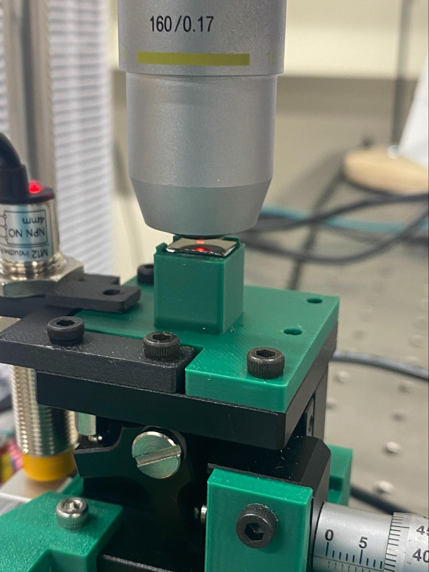
Probe station setup
Probe station - Karl Suss PM5
At least 4 probes, manipulators, and coaxial to split jumper wires with hooks at the end
Microscope setup
Camera - AmScope MU1000-HS and AmScope viewing software
Light – MI-150 Fiber Optic Illuminator
Semiconductor analyzer system
2 Analog Discovery 3s
Laptop with ability to connect to camera and analog discovery 3s as well as run a python program
Materials
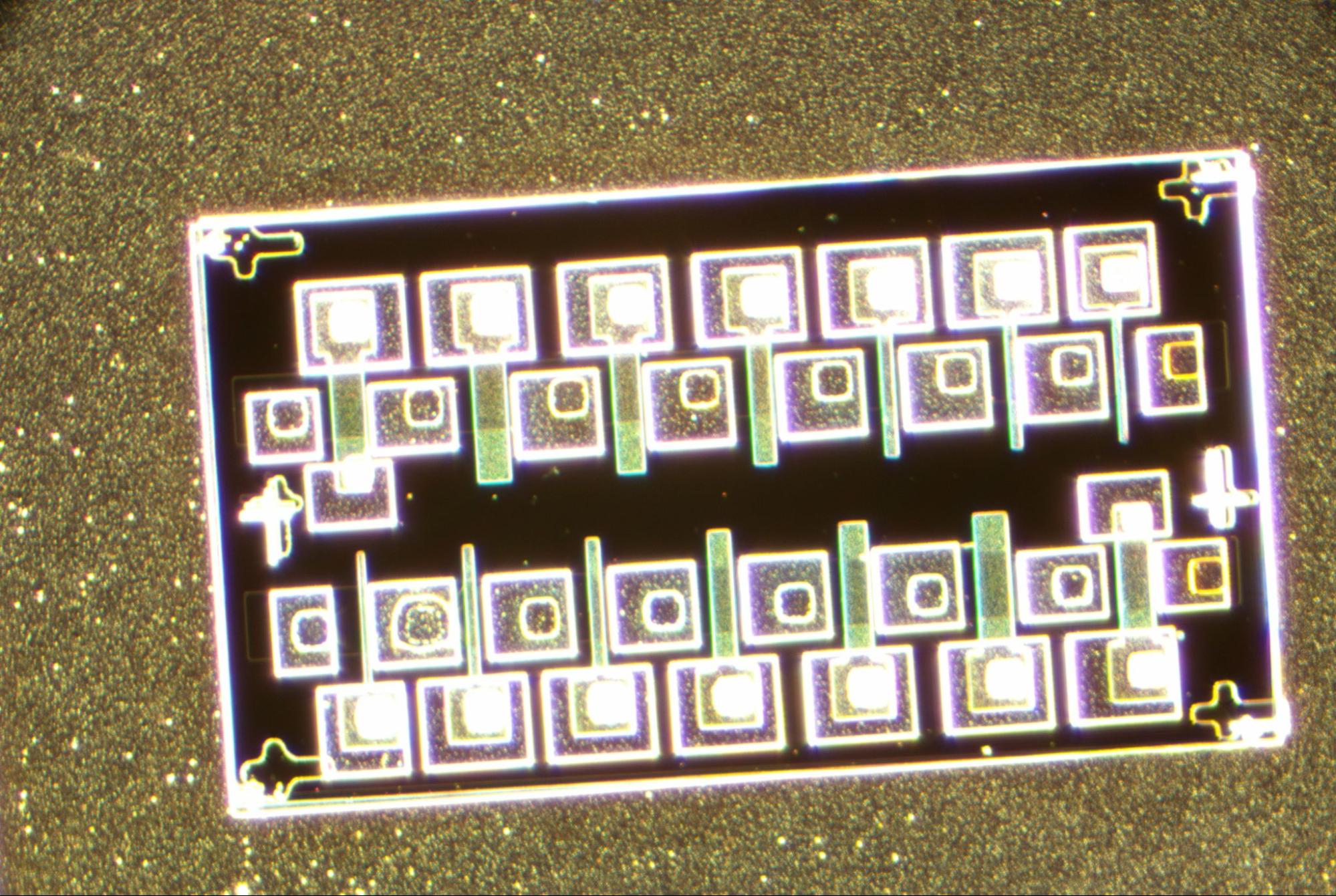
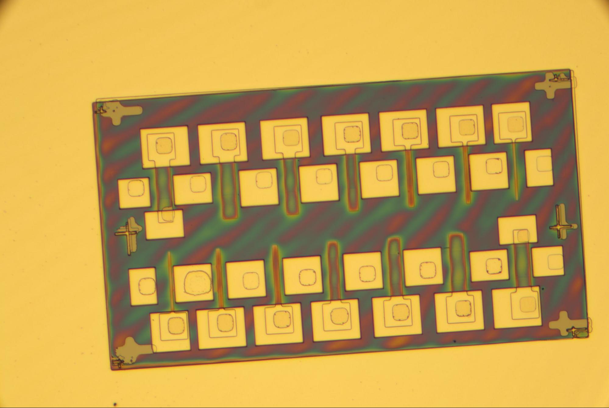
Devices under test – typically a finished chip with pads for probing
Place the chip in the center of the stage and turn on the vacuum.
Turn on the microscope light, which appears as a spot of light on the stage.
Connect the microscope camera to your computer and select the camera MU-1000HS on the AmScope viewer software, which should summon the camera view.
Open the analyzing software on a laptop
Raise the stage using the lever. Focus the stage and center the pattern of interest under the light source using the knobs below the stage.
If the probe tips are not illuminated by the microscope light, carefully move the magnetically-attached manipulators such that the range of motion of the probe tips is within the spot of light.
Using the knobs on each probe’s manipulator, lower the probes so that the tips are focused yet not touching the chip, then position the probe tips above their corresponding probing pads.
Carefully lower the probe tips to touch the pads, which is generally indicated by resistance to movement when attempting to lower the tip further. The manual nature of this process means that the sharp probes can scratch the chip and damage the device beyond future usage, such as scratching the pads off.
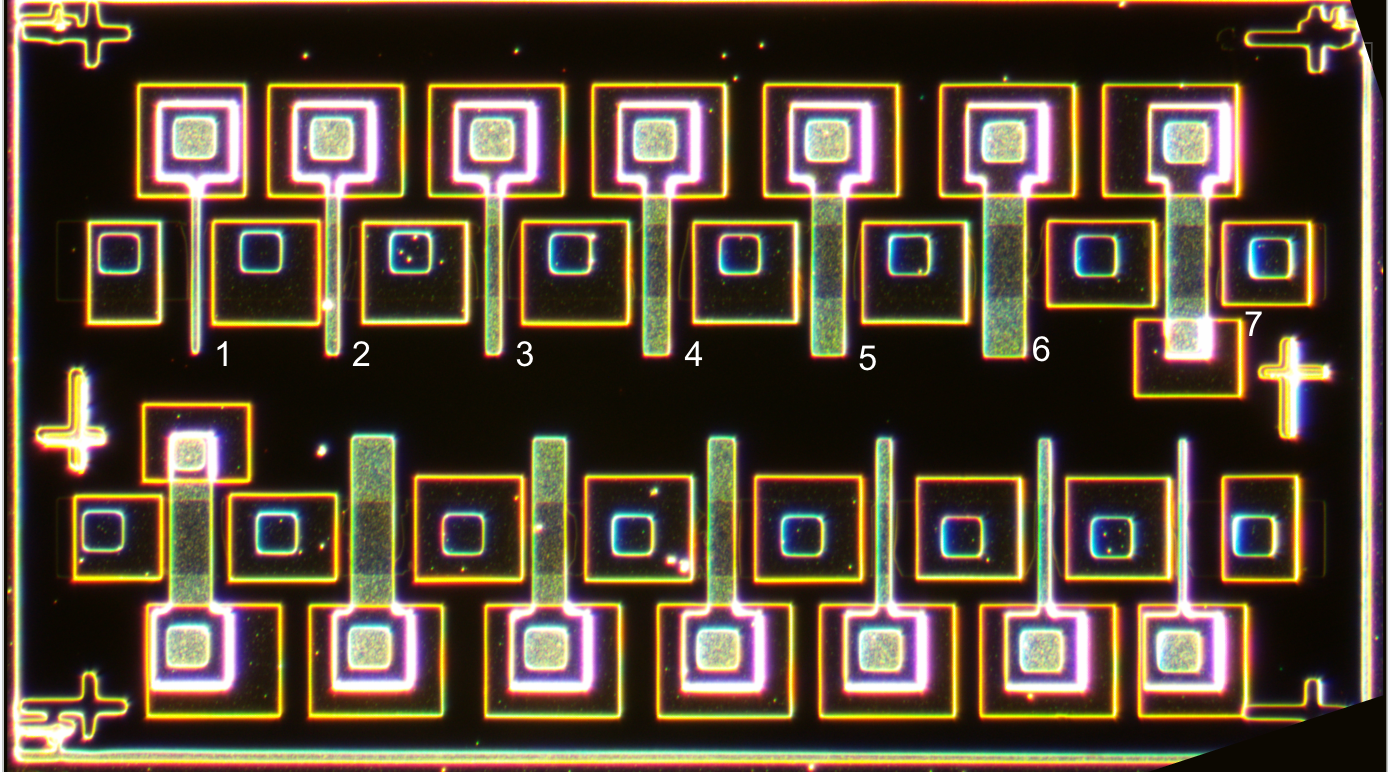
Using coaxial cables connected to the jumper wires with hooks, connect each probe to the ground, source, and drain on the Keithley and connect the corresponding red hooks to the equivalent ground, source, and drain pins on the circuit board as well as all the black hooks to the drain pin on the circuit board like in the below picture
Run Program
Program from Vscode view + terminal
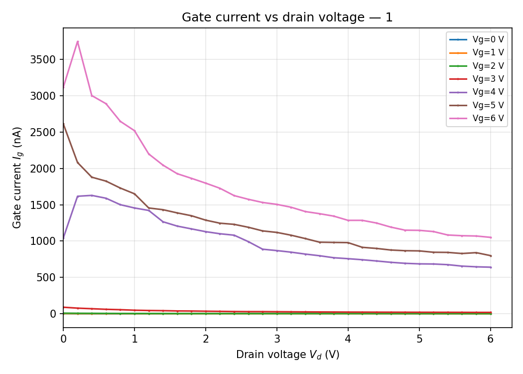
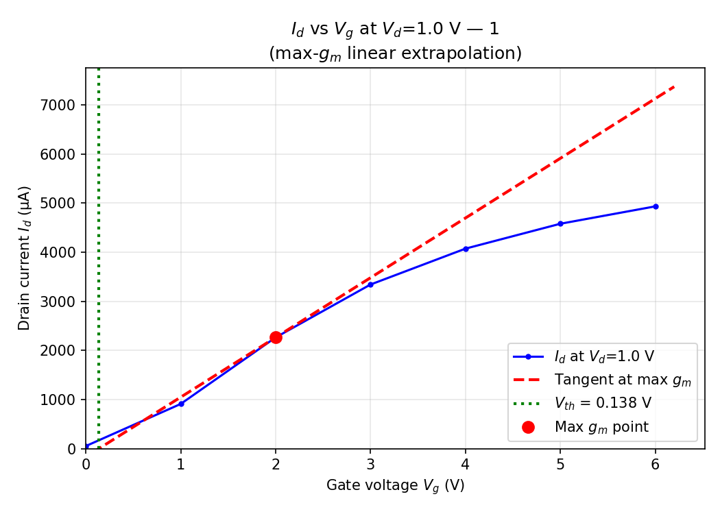
New window with plot of IV curves for ideal mosfet
Run the command python3 smu.py in terminal to run the program
This will open up a new window with a plot of the IV Curve that looks something the below picture under MOSFET I-V Curve
In order to close this window and continue with the program, either hit the red exit button on the image window or go to terminal and type Ctrl-C
If the graph had errors, repeat the experiment as necessary
If the data looks good, enter the title for the current and image csv files
Cleanup
Remove the probes from the chip and continue to the next device, either by lifting the probes or lowering the stage.
Raise the probes using the manipulator knobs.
Lower the stage by turning the lever.
Disconnect the microscope from your computer and turn off the microscope light.
Turn off the vacuum and remove the chip.
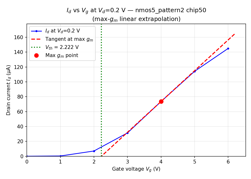
MOSFET I-V Curve
The outputs currently look something like this:
IV Curves for Chip 234 with Gate Voltages of 1, 2, 3, 4, and 5 Volts
The I-V relationship between the two probes and resistance estimated from Ohm’s law should be plotted. An ideal resistor should have a linear relationship and constant resistance.
The ideal goal for the Silver furnace would be to reach 1000 degrees C with around 500 Watts of power, and be able to maintain this temperature for long periods of time without failure. Additionally, this tube furnace should be able to utilize the PID controller successfully to maintain this temperature.
2. Major components
The tube of the furnace is a 2” diameter quartz class tube with 5mm thickness, wrapped in about 3 layers of ceramic wool and held together with metal zip ties. Wrapped around the glass tube is 24g double twisted kanthal wiring, held in place with refractory cement. Surrounding this is a tube of sheet metal held by sheet metal screws and two metal end caps with holes cut through to allow access to the tube and for the wiring to stick out. A stand and handle made out of sewer pipe brackets is included in the design, and attached to the stand is a bracket with a plastic wiring box to act as a space to attach the PID controller, PID relay, and fuse reset. The kanthal wiring that extends beyond the tube is folded in half lengthwise (thickness of 4 24g kanthal wires) and covered in a ceramic weave tube for insulation. The wiring used for the PID and associated devices are recycled wires from an old chandelier, coated in a rubber insulation. Heat resistant tape is used to protect the wires in places where needed. A thermocouple is attached to the PID controller and inserted in the furnace. The furnace is wired to an extension cord and plugged into a programmable circuit breaker to protect the main power grid.
3. Materials
Sheet metal, kanthal wire, refractory cement, ceramic wool, quartz glass tube, nuts and bolts, sewer pipe brackets, ceramic weave wire insulation, motor control, thermocouple, heat resistant tape, voltmeter, programmable circuit breaker, handle, PID controller, PID relay, plastic circuit box, metal bracket, rivets, metal zip ties, fuse reset, metal end caps
4. Construction
1. Coat mid section of glass tube in refractory cement, score lines to allow for shrinkage during curing, let cure for several hours
2. Measure kanthal wire using the desired number of loops around the tube, with some extra length, then double the total length. Fold in half and twist the entire wire tightly using a power drill and tension. Carefully wrap wire around the cemented area of the tube, holding firmly. Hold with rubber bands and cement on top, let cure.
3. Wrap tube with wire in 3 layers of ceramic wool. Bend the twisted kanthal wiring in half to increase resistance and extend to fit where the hole sites in the casing would be. Use ceramic weave insulation and heat resistance tape. to prevent contact between wiring and the casing.
4. Bend sheet metal into a tube and secure together with screws or rivets. Drill holes to allow for wiring to come through the casing. Drill 2” holes through the end caps and secure to the tube furnace with sheet metal screws.
5. Screw on stand, add bracket with holes to the stand and screw the plastic circuit box to the bracket. Pull insulated kanthal wires into the box and wire PID controller, relay, fuse reset, and thermocouple.
5. Testing and performance
Hit the energy and temperature requirements
Still functional after may test runs
Failings with the PID controller, requires the use of the motor control to control the current and prevent the furnace wires from overheating, additionally requires the use of a lightbulb to kickstart the motor control into drawing power and heating using the PID is inconsistent due to the jumps in current.
6. Things to improve on
Need to figure out circuit configuration to power furnace without use of light bulb
Need to figure out how to control current without motor control (for simplicity)
Need to figure out insulation problem for wires to prevent them from becoming too hot
Tube Furnace 3: Tabasco
Goals and operating parameters
The minimum goal to reach with the tabasco iteration of the tube furnace is to reach 1000C with no more than a calculated 1000 Watts of power. The ideal goal would be to reach this temperature with around 500 Watts of power. Maintaining this temperature for long periods of oxidation is also important.
Major components
The tube of the furnace is a 2 inch quartz glass tube, with a center covered in refractory cement, and approximately 20 loops of double twisted 24g kanthal wire wrapped over the cement portion. This is wrapped in several layers of ceramic wool insulation, and then covered with sheet metal. The sheet metal is held together with shelf brackets and a handle. On the back of the tube is an attached thermocouple for temperature measurement. Other parts of the setup include a programmable circuit breaker to protect the local circuit from overloading, a motor control to control the voltage/current flowing into the furnace, and a voltmeter attached to the thermocouple for temperature readings.
1. Coat outer mid section of glass tube in refractory cement, score lines to allow for shrinkage during curing, let cure for several hours
2. Measure kanthal wire using the desired number of loops around the tube, with some extra length, then double the total length. Fold in half and twist the entire wire tightly using a power drill and tension. Carefully wrap wire around the cemented area of the tube, holding firmly. Hold with rubber bands and cement on top, let cure.
3. Wrap tube with wire in ceramic wool. Connect ceramic wiring to the extra kanthal wiring.
4. Bend sheet metal into a box, drill hole to fit tube through as it sticks through insulation. Place the tube through sheet metal box. Drill holes for wires, use ceramic beads to prevent contact between wiring and the sheet metal box.
5. Bracket the edges of the box, leaving extra bracket to allow the furnace to stand up. Fix in thermocouple.
Testing and performance
Successful for oxidation purposes
Can maintain heat for long periods
Despite this, doesn’t hit power goal of 500 W for 1000oC (~1400w)
Things to improve on
Can be more efficient in trapping heat and power usage
Heavy and bulky
Thermocouple could be mounted better
CV Measurements
Capacitance-voltage (CV) profiling is a powerful technique for characterizing semiconductor materials and devices, especially the transistors that we build in our fab. The shape of the CV curve will provide information about the doping concentration in the silicon substrate. On this page, we will detail how to take CV measurements of your devices.
Equipment
Probe station (see here for standard operating procedure)
Capacitance-voltage meter (i.e. Keithley 4200-SCS Semiconductor Parameter Analyzer)
Procedure
Prepare the Transistor:
Ensure that the transistor surface is as clean as possible to minimize probe-to-pad contact issues. It is helpful to have another user with you to properly align and contact the pads without damaging other probes or the transistor surface.
Ensure that the transistor is properly connected and biased for C-V measurements (i.e. for an NMOS transistor, ground the bulk and source contacts, apply voltage from the gate or drain depending on the type of measurement).
Measurement Setup:
Set up the CV measurement equipment, we use a Keithley 4200-SCS Parameter Analyzer as our test equipment and Probe Station for circuit connections. Please follow the steps given in the to ensure proper probe-to-pad contact with the transistor.
Voltage Sweep:
If using an NMOS transistor with 3 terminals (i.e. no bulk contact), turn off the bulk probe on the KITE interface, ground the source pad, apply a small-signal AC voltage to the drain pad (constant frequency ideally above 100 Hz, low frequency measurements will be performed later), apply a large-signal DC voltage sweep to the gate pad (-8V to +8V for our case). Measure the total capacitance from the gate pad as well. If your NMOS transistor has a bulk pad as well, it is possible to modulate the bulk potential and model threshold voltage dependencies. For regular use, grounding the bulk and/or at least having it at the same potential as the source pad is ideal.
It is also possible to model the MOSFET as a MOS capacitor instead by connecting source and drain to the ground and only by sweeping the gate voltage. This “topology” may be deemed ideal to extract capacitive parasitics from the measured total gate capacitance:
Plotting CV Curves: Plot the measured capacitance as a function of the bias voltage. Below is an example of a measured capacitance versus applied voltage (C-V) curve. Note the decrease in the total capacitance as the mode of operation changes from accumulation in the deep negative voltages to depletion as the capacitance decreases significantly. There is no bulk contact in this measured NMOS transistor, and therefore the inherent and uncontrollable modulation in the bulk potential may be preventing the change of the mode of operation from depletion to inversion (note the lack of increase in the capacitance as the gate potential approaches +8V).
Analyzing C-V Curves: The shape of the CV curve will provide information about the doping concentration in the silicon substrate.
Dopant Concentration (ND): To measure the concentration of the deposited donor atoms, either the source or the drain terminal of the NMOS is used with respect to the bulk. If the drain and the gate are grounded, the subsequent capacitance measurements will be done between the bulk and the source terminals. Since the source and the bulk regions are oppositely doped, they form a p-n junction with a depletion region in between. This structure presents inherent diode and capacitive properties, which is ideal for doping concentration and profile measurements. The average doping should be extracted to later calculate the Debye length (in plasma physics, the distance at which a charge (among a sea of other charges) is shielded against electrostatic forces of a charged plane, such as that of a capacitor), flat band capacitance and bulk potential.
Flatband Voltage: Flat band voltage is the voltage that must be applied to the gate terminal at which the metal-oxide-semiconductor interface potential becomes equal in magnitude to the built-in potential, making the surface potential zero. Since the presence of a flat band condition affects the accumulation of charges for accumulation or inversion channel formation, it is an important parameter to extract for the modeling of the threshold voltage. VFB is usually interpolated from the C-VGS curves, if and only if the doping profile is assumed to be uniform over the region and interface trap state density is large. Otherwise, measuring the flat band voltage is finicky at best and extremely difficult at worst due to our fabrication methods.
Model Fitting: As a general rule of thumb, for long-channel devices such as ours, 1 MHz is the frequency at which high-frequency measurements are performed, while low-frequency measurements are generally performed at and below 100 kHz, down to 1-10 Hz.
Use semiconductor device simulation software or a theoretical model to fit the experimental CV curve to theoretical curves, which depend on the doping concentration. This can provide a more accurate estimation of the doping concentration. See the ideal CV curve below:
Extract Parameters: From the fitting or analysis, extract parameters such as doping concentration, and threshold voltage using known parameters such as oxide thickness. See page 10 of for a detailed explanation of the relevant equations. has an implementation of those equations in MATLAB.
Future Work
As of June 2024, we are currently working on our own custom probe station and source-measurement unit, as described . Once this is complete, we will be able to use our new setup to take CV measurements. We will update this page accordingly once this is done.
Reference Sources
Tube Furnace SOP
Doped Silicon (grey) and Doped Gate Poly (dark blue) Resulting from Thermal Diffusion
Tube Furnace
Parameters
Temperature
generally 1100°C
Purpose
The primary use of the tube furnace is for diffusion of dopant atoms into silicon. The incorpoation of dopant atoms into the Si lattice creates defects in the electronic structure, which are charge carriers, increasing the conductivity of the diffused region and making it either N or P type. Diffusion of a solid into another solid is quite slow, so high temperatures and long times are needed, hence the high-temperature tube furnace.
Our process uses spin on glass containing phosphorus for N doping and boron for P doping.
Tools
Tube Furnace () with Quartz tube
Quartz rod
Quartz microscope slide, or Fused silica boat
Materials
Chip with glass containing phosphorus or boron.
Procedure
Pre-heating the Furnace
Turn on the furnace.
Press and hold “set/ent” for three seconds until “mode res” is showing. Press the up arrow twice until mode “LCL” is selected. Press “enter” once. Now the furnace will hold the temperature shown. Use the arrow keys to adjust and press “enter” once to set the setpoint.
If the furnace stops and holds at a lower temperature than your setpoint, the high temperature alarm may be too low. Read the instructions on to fix this.
Inserting chips
Put the Quartz microscope slide in the entrance of the tube. Do not use a regular borosilicate microscope slide, or it will melt inside the tube. The edge of a fused silica slide is pure white, while borosilicate is a little bit green.
A chip permanently fused to the tube furnace walls when improper slide was used 🔥
Place your chips on the slide.
Put on the heat resistant gloves.
Use the glass rod to push the slide into the center tube, being careful to not scratch the inside of the tube too much
Removing chips
Use the glass rod to push the slide to the other end of the tube.
Wait a few minutes for the slide to cool down.
Use metal tweezers to take the slide out. place it on the upside down beaker to allow it to cool further
Safety
The furnace is obviously very hot. Keep away from any hot parts of the furnace. The rod will heat up in the few seconds that it is inside the tube, so when removing it, only hold it by the colder end.
The rod and tube also channel heat out of their ends via internal reflection of radiation.
Spin on Glass Thickness Measurement
*This only works with SoG on pure silicon and NOT polysilicon. Should work for both 700B/P5O4
Purpose
The main purpose of this SOP is to describe a method that we can use to approximate the thickness of SoG. This is especially important in certain plasma etching processes, where removal of SiO2 is needed.
Tools
Spectrometer
Spectrogryph opened on computer connected to microscope view
(should end with .sgd, can only be opened in the Spectrogryph app)
Picture of Spectrometer Below:
Materials
Silicon Chip with 700B/P5O4 SOG
Steps
Setting up the software + obtaining spectrometer data
First, ensure that the spectrometer is connected to the computer.
In addition, place SoG on silicon chip sample on the slide under the microscope.
Open Spectrogryph software on Computer
Under Plot/Views, select “New Acquisition View”
After which, you should see something that looks like:
In the upper left corner, select “Device Type” and select ASEQ. Then press connect.
Change exposure to 5000 ms (or more, if you want less noisy data)
Select single shot or continuous
7. Once a graph of Count against Wavelength is obtained, we need to normalise the counts. This is done by clicking on "Process" and "Normalise (Peak)".
Once normalized, we can now save this spectral plot in file (save it in the .sgd format, so that you can re-open it in spectrogryph later)
Determining Thickness of SoG
Create another New Acquisition View
Drag the (should end with .sgd) into the New Acquisition View
You should see this:
The color of the graphs correspond to the actual observed colors of the glass. This can serve as a good benchmark as to what the thickness of your glass might be.
As seen, the SoG with the lowest thickness (190 nm) had the maximum peak at a wavelength of ~590nm. As the glass thickness increases from 190 nm to 255 nm, the wavelength at maximum peak increased accordingly. Following that, from 255 nm to 276 nm, it can be seen that a second peak is starting to form (at a wavelength of around 480 nm). Finally, from 276 nm to 314 nm, the peak at 590 nm disappears, and now the peak at 480 nm becomes more distinct.
Lastly, drag the .sgd file that you previously saved in Step 7 into the plot above.
Determine which shape your graph most closely resembles to determine SoG thickness.
Also note that the color of your glass is a pretty good indicator of what thickness it will be. So for instance, if your chip looks pink, just by looking at the calibration graphs, we can determine that thickness is around 270 nm.
Useful Links
Spectrogryph Manual Website:
Profilometer SOP
SOP for using the profilometer
Purpose
The purpose of the profilometer is to measure the roughness of a surface. Specifically, it is able to measure height differences across a region of interest (in one dimension) in the nano scale. This is useful especially after etching processes, where we can measure how much etching was performed on the chip.
The precision of this instrument is ~20-30 nm.
Materials
Profilometer
Your chip
If you are learning how to use the profilometer and do not have any patterns yet, you can use Chip 365 (there is a pattern on it, and it is also used in this tutorial)
The profilometer (right) is connected to a very old computer (left). The profilometer contains a metal needle tip that is used to measure the roughness of a surface.
Procedure
Place chip on stage
Ensure that you don't place the chip in the ridges, and this can lead to a runtime warning
Switch on the light on the stage, ensure that chip is under the light
On computer, go to Display > Video to visibly see the chip. Also, select Sample Positioning in order to see where the stylus will start measuring.
Move chip until you are able to see the cross hair being in line with the edge of your patterns.
Chip can be moved using the knobs as seen in Figure 2.
Ensure that you don't touch/bump into the metal tip as it is very sensitive and delicate
Go to Run > Run Single Scan to start an experiment. The stylus will start moving.
If it runs into the AD conversion error, keep retrying (the error tends to go away after 5-6 times, see bottom of this document for photo)
Results and Data Analysis
After the run is completed, this should be seen:
As seen in the Figure above, we can see two "bumps", which are where we want to collect our data. However, we can also see that the graph is slanted, which means we first need to level our data.
Levelling plot: Move the red and green vertical lines such that in between those lines, we have a relatively flat region (as seen in Figure 6). Go to Plot> Level. We should now see this:
In order to measure the step height, drag the red and green vertical lines such that in between these lines we have the region of height difference (shown in Figure 7). The height difference is captured as Vert_D. In this case, we an see that it is 2425 Angstroms, which translates to around 243 nm.
Other Features
As seen in Figure 7 above, some regions are "bumpy". In order to get the average of these "bumps", one can go the Bands > Create Band and set a specific distance. For instance, in Figure 8 below, we have taken the average of 50 nm to the left and 50 nm to the right of the region of interest.
Errors that might occur
1) Timeout Waiting for AD Conversion
This error happens very often. In order to fix this, perform multiple runs (usually around 5-6 times) until the timeout notice is no longer shown.
Patterning
For a description of what the team at CMU is working on in Spring 2025, check out !
Goals of this page:
Not to try and cover theory or industry standard, but to break the problem into first principles just enough to give context to the quantifiable parameters
Also an opportunity to frame the problem wide enough to set the tone of thinking of these machines from the ground up (aligned with goal, don't think of industry as immutable)
Tube Furnace 5: Flame
Scanning Tunneling Microscope
Fall 2025 documentation @ CMU
Development Log — Tip Etcher - Replicable Progress with Unforseen Challenges
Database
Overview
The Hacker Fab was built on the Django framework using Python, with HTML and CSS serving as the front-end. The code in this . The purpose of the database is to store data related to chip fabrication in our labs and use the results to refine our process parameters. It is crucial that we maintain a comprehensive and functional data store in order to develop new processes and to help new Hacker Fabs begin fabrication.
The database was created in Spring 2024 with the ability to create new chips, add process parameters to each chip, and query back results from the database. The front-end had simple styling, although they were not reflected in the production website due to issues with certification. The motivation for our improvements in Fall 2024 was increasing the intuitive usability of the website, as well as adding more functionality for the user. hi
Thermal Evaporator SOP (CMU Version)
Materials
Procedure
Probe Station SOP
Purpose
After fabrication, the chip must be tested to demonstrate the functionality of the design. Additionally, variations and errors in fabrication may result in differences in device characteristics which are useful to document when these variations cause the device to fail.
To enable precisely controlled experiments on microscopic chips, we currently use a probe station to contact the device using sharp probes which supply and measure voltages for calculation of various device characteristics such as I-V curves, which are explained in this SOP.
Aluminum Etch SOP
Parameters
Cut Brackets
Approximately 5’8” of bracketing used, each bracket side is 1” wide with about 4 mm thickness, additional half bracket bar was cut to hold the handle going across
Go to Stylus > Stylus Down. This will move the stylus down to the chip and it should be aligned with the cross hair.
If the stylus is not aligned with the cross hair, double click on the new location where you want the cross hair to be. You will be prompted to update the cross hair location.
Figure 1: Profilometer Set Up
Figure 2: Profilometer Setup Movement
Figure 3: Display > Video and Display > Sample Positioning
Figure 4: Display > Sample Positioning shows where the cross hair will appear
Figure 5: What you should see after Stylus Down command
Figure 6: Results from Profilometer Run
Figure 7: Levelled Results from Profilometer
Figure 8: Using Bands when analyzing data
Figure 9: AD Conversion Error
Approximately 8’ of bracketing used, each bracket side is 1.5” wide with about 2 mm thickness
Glass used was too thin
Item
Specifications
Quartz Glass Tube
14” long, 2” diameter, 2 mm thickness
Sheet Metal
Folded into a 9.5” x 9.5” x 10.5” box
Kanthal Wire
24g, 20’+, wrapped into 20 loops around glass tube
Ceramic Wool
1” thick, cut to wrap once around the tube and to wrap around refractory bricks 5” x 5” x 1” refractory bricks
Thermocouple
8” long, mount has less than 2” diameter
Refractory Bricks
5” x 5” x 1” each, 2” hole cut through middle for glass tube, approximately 5 used and held together by refractory cement
Shelf Brackets
Circle diameter of around 5”, adjusted using bolts to fit the furnace snugly
Despite this, when the current is controlled with the motor control, the PID controller works effectively in maintaining a specific heat in the furnace
Item
Specifications
Quartz Glass Tube
9.5” long, 2” diameter, 5 mm thickness
Sheet Metal
Folded into a tube of 8.5” length and 5” diameter
Kanthal Wire
24g, 20’+, wrapped into 20 loops around glass tube
Ceramic Wool
1” thick, cut to wrap 3x around the glass tube
Thermocouple
6” long, mount has less than 2” diameter
Metal End Caps
5” diameter to fit around sheet metal tube, with a 2” circle cut in center to allow for access to glass tube
Programmable circuit breaker to protect the power grid and voltmeter for thermocouple readings
PID and Relay setup
Sewer Pipe Brackets
When in accumulation (VGS < 0), mobile holes from the p-type substrate form a dielectric region due to being attracted under the gate. The total gate capacitance is the sum of the gate-source and gate-drain overlap capacitances, along with the gate-bulk capacitance.
When in depletion (VGS is a small but positive voltage), some number of mobile electrons are attracted under the gate but not enough to fully invert the net channel charge, therefore the region under the gate simply becomes devoid of mobile charges, but becomes more negative as the gate voltage is increased. Total capacitance is the sum of the overlap capacitances (which are often neglected due to their small magnitude) and the oxide capacitance (between the gate oxide and the induced weak negative channel) in series with the depletion region capacitance. This parallel topology decreases the total capacitance.
When in inversion (VGS >> 0, much larger than the threshold voltage required to “turn on” the MOS), a substantial number of electrons are attracted under the gate such that a strong conduction channel forms. The conduction channel forms the bottom plate of this virtual capacitance, and the distance between this bottom plate and the gate decreases as the channel inversion becomes stronger (with increasing gate-source voltage), increasing the total capacitance. Apply a DC voltage sweep to the transistor, typically from negative to positive bias (usual measurement range is from -8V to +8V). Measure the capacitance at each bias voltage.
Metal-Semiconductor Work Function Difference: The work function difference is a key parameter in determining the threshold voltage of the MOS transistor since the WMS forms a potential barrier against the inversion of the channel. The bulk potential, which is extracted using the doping profile, is an input to WMS.
Use Single Shot if you want to get one graph that is taken after 5 seconds of exposure
Use Continuous if you want a graph that is constantly being recorded (hence changing)
Pressing “Acquire” would start the readings. Before pressing “Acquire”, ensure that the probe is connected to the microscope (will need to press the probe against the microscope to get good readings, as shown in picture below).
Quantifiable end user parameters with descriptions + standardized tests
Background
Overview
A photolithography stepper is a machine that exposes a pattern of light onto a layer of photoresist chemical on the wafer, then ‘steps’ over to the next pattern. Before each exposure, it must align with previous patterns on the wafer so that each layer of the device is in the correct position relative to the previous. The accuracy with which it can do this is called “alignment accuracy”. Alignment accuracy and optical resolution are the two most important metrics of a stepper’s performance.
There are 2 main components of our stepper: the light source and optics, and then the mechanical micropositioning stage that moves the chip itself. Alignment accuracy is a function of both the mechanical micropositioning stage and the reliability of the projector’s optomechanical components.
Masked vs. Maskless Lithography Systems
Commercial lithography machines use photomasks to create the image, typically made of chrome on glass. Instead, our Maskless Photolithography Stepper uses a DLP projector to create a pattern. This allows us to change patterns instantly, opening the option up for advanced techniques like tiling (making a circuit larger than one exposure field).
Quantifiable Parameters
Functional Specifications: The End Product
Developed Resolution
describe out standardized test: darkfield/brightfield, developed with AZ400K for 80s, measured pitch distance, used airforce test pattern
Value:
Tools Required for Verification:
Method of Verification:
Possible Variation: Error during development (see )
References: pics/videos
Automation Capabilities / Throughput
what human actions are required: manual loading/unloading, choose the pattern, align manually or automatically with software
approximate area exposed per second
how much time to do one exposure, how much of that is active work vs. waiting around
Patterning Machine Specifications:
Optical Resolution
Tools Required for Verification: Microscope + Calibrated Camera to convert pixels to μm
Method of Verification: make another page for optical resolution test?
Possible Variation: misalignment of optics during assembly
References: pics/videos
Developed Resolution
Tools Required for Verification:
Method of Verification:
Possible Variation: Error during development (see Patterning SOP)
References: pics/videos
Single Exposure Area
Approximate Exposure Time (for AZ P4210 photoresist)
Tools Required for Verification: AZ400K Developer Solution + Microscope
Method of Verification:
Possible Variation: Can vary UV LED power and beam splitter ratio to decrease/increase exposure time
The ideal goal for the Flame furnace would be to reach 1000 degrees C with around 500 Watts of power. Maintaining this temperature for long periods without oxidation of wiring is also important. Furthermore, this design needs to be durable and operational for multiple trials. An additional goal is to set this furnace up with a PID (Proportional Integral Derivative) controller to control the maximum heat of the furnace.
Major components
The tube of the furnace is a 2” diameter quartz class tube with 5mm thickness, wrapped in about 3 layers of ceramic wool and held together with metal zip ties. Wrapped around the glass tube is 24g double twisted kanthal wiring, held in place with refractory cement. Surrounding this is a tube of sheet metal held by sheet metal screws and two metal end caps with holes cut through to allow access to the tube and for the wiring to stick out. A stand and handle made out of sewer pipe brackets is included in the design, and attached to the stand is a bracket with a plastic wiring box to act as a space to attach the PID controller, PID relay, and fuse reset. The kanthal wiring that extends beyond the tube is folded in half lengthwise (thickness of 4 24g kanthal wires) and covered in a ceramic weave tube for insulation. The wiring used for the PID and associated devices are recycled wires from an old chandelier, coated in a rubber insulation. Heat resistant tape is used to protect the wires in places where needed. A thermocouple is attached to the PID controller and inserted in the furnace. The furnace is wired to an extension cord and plugged into a programmable circuit breaker to protect the main power grid.
Materials
Sheet metal, kanthal wire, refractory cement, ceramic wool, quartz glass tube, nuts and bolts, sewer pipe brackets, ceramic weave wire insulation, motor control, thermocouple, heat resistant tape, voltmeter, programmable circuit breaker, handle, PID controller, PID relay, plastic circuit box, metal bracket, rivets, metal zip ties, fuse reset, metal end caps
Item
Specifications
Quartz Glass Tube
11.5” long, 2” diameter, 5 mm thickness
Sheet Metal
Folded into a tube of 10.5” length and 6” diameter
Kanthal Wire
24g, 20’+, wrapped into 20 loops around glass tube
Ceramic Wool
1” thick, cut to wrap 3x around the glass tube
Thermocouple
6” long, mount has less than 2” diameter
Metal End Caps
6” diameter to fit around sheet metal tube, with a 2” circle cut in center to allow for access to glass tube
Construction
1. Coat mid section of glass tube in refractory cement, score lines to allow for shrinkage during curing, let cure for several hours
2. Measure kanthal wire using the desired number of loops around the tube, with some extra length, then double the total length. Fold in half and twist the entire wire tightly using a power drill and tension. Carefully wrap wire around the cemented area of the tube, holding firmly. Hold with rubber bands and cement on top, let cure.
3. Wrap tube with wire in 3 layers of ceramic wool. Bend the twisted kanthal wiring in half to increase resistance and extend to fit where the hole sites in the casing would be. Use ceramic weave insulation and heat resistance tape. to prevent contact between wiring and the casing.
4. Bend sheet metal into a tube and secure together with screws or rivets. Drill holes to allow for wiring to come through the casing. Drill 2” holes through the end caps and secure to the tube furnace with sheet metal screws.
5. Screw on stand, add bracket with holes to the stand and screw the plastic circuit box to the bracket. Pull insulated kanthal wires into the box and wire PID controller, relay, fuse reset, and thermocouple.
5. Testing and performance
Hit the energy and temperature requirements
Still functional after may test runs
Failings with the PID controller, requires the use of the motor control to control the current and prevent the furnace wires from overheating, additionally requires the use of a lightbulb to kickstart the motor control into drawing power and heating using the PID is inconsistent due to the jumps in current.
6. Things to improve on
Need to figure out circuit configuration to power furnace without use of light bulb
Need to figure out how to control current without motor control (for simplicity)
Design can always be more energy efficient
Programmable circuit breaker to protect the power grid and voltmeter for thermocouple readings
PID and Relay setup
10/19/2025
Cathode Ring Issue
• Discovered that the stainless-steel cathode ring arrived slightly deformed from shipping, causing improper fit in the provided glass beaker.
• Attempted reshaping; glass beaker cracked during refitting.
• Contacted Baird Labs — vendor acknowledged issue and shipped replacement ring and beaker with looser tolerance for future customers.
Ring Fabrication Contingency
• For other hackers, here is a fabrication procedure if unable to procure replacement from vendor and issue persists:
1. Measure inner circumference of electrolyte beaker.
2. Cut stainless-steel strip slightly longer than circumference.
3. Use ring roller to form consistent curvature.
4. Spot-weld overlap to close the loop and ensure conductivity.
10/24/2025
Replacement Ring + Glass Beaker Arrived
10/26/2025
Calibrated Tip Etcher
• Followed Baird Labs Calibration and Tip Etching Demo:
• Used Oscilloscope found in Hacker Fab
• Determined Cutoff Voltage to be 1.5V and Etching Voltage to be 12V using methedology presented in video and presented here:
11/09/2025
Etched Atomically Sharp Tips
• Followed our Hacker Fab Authored "How To Etch a Tip" Manual, integrating an Analog Discovery 3 and a laptop for repeatable etching. Full Steps outlined here:
11/10/2025
Characterized Atomically Sharp Tips
• Imaged our Tips using CMU MCF, discerned an upper bound on sharpness to be below 50nm in tip radius.
Development Log — Positioning System - Replicable Progress with Unforseen Challenges
Date
Item / Notes
09/08/2025
Hardware Procurement
• Created and finalized the , listing all required fasteners, aluminum, and piezo actuators.
• Ordered all parts from vendors that sell into the U.S. market, including McMaster-Carr and Digi-Key.
10/05/2025
3D Printing — Shell and Shell Cover
• Printed the shell and shell cover in PLA on a Bambu X1 Carbon while awaiting shipment of mechanical parts
• STL files: , .
• Shell: Grey PLA — 215 °C nozzle / 50 °C bed, 30 % infill, brim adhesion, 43 min.
• Shell Cover: White PLA — 200 °C nozzle / 60 °C bed, 10 % infill, brim adhesion, 50 min.
Printing Issue and Remedy:
• Slight corner warping observed on the shell-cover; plan to increase bed temperature to 55 °C and widen brim adhesion in future prints.
11/10/2025
Reprinted Shell and Shell-Cover
• Printed the shell and shell cover in PLA on a Bambu X1 Carbon while awaiting shipment of mechanical parts
• STL files: , .
Used what we learned about settings from our attempt on 10/05/2025
12/01/2025
CNC'd the Aluminum Components
• Printed the alumunum components found here:
Date
Item / Notes
09/08/2025
Purchase Order
• Contacted BairdLabs via WhatsApp and placed an order for the Simple Tungsten Tip Etcher Kit
09/29/2025
Assembly
• Received shipment from BairdLabs LLC
• Assembled Baird Labs Simple Tungsten Tip Etcher kit following official build-guide video from bairdlabsllc.com.
Build Guide:
• Full Assembly completed. Kit included all necessary mechanical and electrical components—no additional parts required.
Design Choices
Web Hosting Platform
The website hosting options up for consideration were Amazon Web Services (AWS), Google Cloud Platform (GCP), and Microsoft Azure. AWS was ultimately chosen because it had the longest free period and we had the most experience working with it. We use EC2 because it has the most flexible options and high availability in many geographic regions. The website is not very compute-heavy, so we chose a small instance to keep costs down.
Model/Schema Changes
The code has a model-view-controller (MVC) structure. Each fabrication process is described as a model (in models.py), with each field representing a process parameter or documentation artifact. This translates to each process being stored as a separate table within the database. This semester, the models were updated to constrain parameters to specific data types in order to maintain consistency and correctness in the database. For instance, temperature was stored as a decimal value, duration as a positive integer, and material type as a string. Some models and fields were renamed as well in order to clarify their meaning. We worked closely with the process development teams to understand which fields should be included or what new models should be added. Relevant Django documentation: Models
In order to allow the user to interface with the database, there are input and search forms based on the models (in forms.py). As of this semester, the input forms require certain parameters that are measurable and critical to the fabrication process, as well as prefilled default values for standardized parameters in our primary NMOS process. The search forms do not have any required fields, since we should be able to search process data for every chip and parameter value. This semester, the search forms were also updated with input fields that would provide users with the ability to perform searches given a specified range of values. The labels to these forms were also refined to be more readable and include units to aid in correct input. Relevant Django documentation: Forms based on models
User Interface
We identified that a non-intuitive workflow and lack of visual cohesion were affecting the usability of our website. One major change was the inclusion of “chip pages” that show every process done to a chip and eventually will allow for edits to the data associated with it. Previously, the only way to see that data was to search the database by chip number. This process was not intuitive because users are usually working with a single chip at a time, so it made more sense to have a centralized location to view that relevant information.
A change for the search page was the use of horizontal tables to display data for a process. In other words, for a single entry, each column represents a certain field in that entry, and each row is a distinct entry (previously, the first column was the field name, the second column was the value, and additional fields for a given entry were displayed in their own row). The horizontal table display makes it much easier for users to distinguish between different entries for chip information and process parameters. Furthermore, we modified the search page to display all filter categories to the user under an umbrella “Advanced Search” dropdown. This allows the user to see all the search options at once instead of having to submit a process. Lastly, to make it easier for users to interpret the data that is presented to them in the search page, we added functionality that allows users to group the search results either by the process types they have selected, or by the chip number.
The chip creation page will also have the option to use a “chip profile” or “chip default” that prefills parameter values associated with an established process, such as the NMOS process we use for class labs.
An important addition to the Patterning process in particular is the ability to add multiple patterns in the same step and click on a gray rectangle to approximately note the location of that pattern. This way, it is easier to record the application of multiple patterns at the same time as well as locate a specific pattern when returning to the chip.
Main Controller
The different web pages in our website are served by their own controller functions which are located in views.py. We designed the backend architecture to have a separate function that serves each unique web page. This design allows us to modularize our backend logic and isolate functionality to those specific pages so that they can be as customizable as possible. If similar logic is used across different web pages, we put this logic in helper functions to avoid having duplicated code. The different controller functions for each page serve the main functionality of our website. Routes between the addresses to these pages and the functions that serve them are specified in urls.py. The controller links the different HTML pages together, performs the database operations, and interfaces with the backend. It determines what form to display based on what process the user selected, saves the form data and passes it to the database after cleaning, displays search queries by the user, and renders the web pages.
Main Controller: Querying Data
As our website serves to display database entries to our users, a crucial functionality is querying data (related to process parameters and chip information) and rendering it on the page. These are the different pages where data querying is critical:
Page Name
Page Address
Controller (Function Name)
Search Page
/search
search_page()
Central Chip Page
/central
central_action()
Chip Page (for a single chip)
/chipnum/<chip_id>
display_chip()
When a user performs a search for data, they can enter specific filters to narrow down their results. These filters are passed to our controller when the user fills out a search form filled with parameter values. In our controller, we use Django’s Q() objects from their database querying library to create and execute SQL queries. This simplifies the process of extracting data from our database since we just need to create a Q() object using the filters specified by the user then apply the filter on our models. This querying is done in the function filter_form(). Data querying is one of the most computationally intensive components of our database; hence, it can be considered as a bottleneck. Querying data for a single model (i.e. process type, user profile, etc.) has a worst case complexity of O(M), where M represents the number of rows that exist for a particular model in our database (the total number of unique entries of that model stored in our database). In the search page, the user is able to conduct a search to retrieve data from multiple process types. In this case, the worst case complexity for the search is O(P*M), where P represents the number of different processes the user has selected, and M represents the number of rows that exist for a particular model in our database.
The code in views.py is responsible for passing the data from the query result to the html files so that they can be displayed on the web page. There is an important detail that developers should take note of when implementing any functions that return queried results to users. We have implemented a specific data format to pass to the html page in order to standardize the design of the html pages and controller function outputs. When an html page is rendered, views.py provides it a context, which contains data (variables) that are required by or will be displayed in the html page. The html page expects the queried data provided in the context to be an array of arrays of dictionaries. Since Django’s querying library returns the queried data to us in the form of a QuerySet, we must convert the QuerySet into an array of dictionaries using Django’s model_to_dict() function found in their forms.models library. Each dictionary represents a single entry in the database. The keys correspond to the column names, which map to the corresponding value for that column. Each array of dictionaries within the outer array corresponds to a grouping of data. This enables us to group data based on the process types so that they can be displayed on the page with the correct column headers. This data structure is depicted below.
Diagram representing the data structure of the query results passed as a context to be rendered in the html
!!!!!!!!!!!!!!!!!!!!!!!!!! System architecture for interfacing with tools (the spincoater for now) !!!!!!!!!!!!!!!!!!!!!!!!!!!!!!!!!!!!!!!!!!!!!
SEE this link for better formatting: https://docs.google.com/document/d/1SrD66bqmS1xxs2jt_WWSY7eLr6vyDJxIB4dbMdbxkws/edit?tab=t.0#heading=h.ai1m6262yla9
Put on nitrile gloves to prevent contaminating the chamber.
If the Pfeiffer turbo pump is on, power it off by pressing the button pictured below.
Use the arrows to scroll to parameter 309, which show pump speed.
Wait until the pump speed is at 0Hz
Slowly vent the chamber by unscrewing the vent screw located on the turbo pump.
Wait until the pressure is at 1E3 hPa or greater (pressure is given by parameter 340, scroll to it with the arrows).
Unscrew the two black knobs pictured below, then lift the chamber lid.
Turn the two black knobs on the top of the blue box as shown above and open the lid.
The tungsten filament is secured with two barrel connectors pictured below. The filament can be removed by slightly loosening the screws closest to the filament.
Tightly wrap aluminum wire near the center the Tungsten coil, you only really need an inch of wire. Due to the alloying between Al and W, the filament becomes more brittle after each evaporation, so be careful not to break it. If you do break it, use a new filament. You may have to use clippers to shorten the ends of the new filament to get it to fit right.
Place the tungsten filament back and screw it in. Make sure it is straight.
Place ~ 1 inch of polyimide tape on the substrate holder shown below, then peel off the clear layer on top of the tape. Since aluminum often covers the square box, when you put the tape on, aluminum might stick to it and flake off. Just continue attempting to apply tape until it stick without flaking off.
Must be polyimide/Kapton tape, otherwise it will outgass under vacuum.
Place your chip on the tape, and use tweezers to gently press down on the corners of the chip.
Double check that the wire and barrel connectors are suspended and not touching anything conductive (including the chamber).
Close the blue lid and screw the black knobs all the way.
Close the vent all the way (hand tight)
Turn on the pump. Monitor the pump speed in Hz. Often, around 270Hz, it makes a bad noise and stops speeding up. This can be resolved by quickly tuning the pump on and off, with the button on the right. It will slow to ~ 160, then re speed up, and pass the point it got stuck at. This is not normal pump behavior, and we are looking into a repair.
Screw the black knobs more since they tend to loosen after the pump turns on.
Wait for the pressure to reach 3.71E-5 torr (lower limit of the Pirani gauge). This may take hours. However, with this system, very conductive films have been deposited at a pressure of only 1E-4 torr when there was a bad seal. If you choose to do this, you are sacrificing some film quality.
Turn on the water cooling for the QCM sensor head. Off is when both handles are vertical, on is when both handles are horizontal.
On
Off
Turn on the hp laptop, and open the STM-2 software. under the STM-2 tab, it should show a connection to a sensor. Then, the frequency value should read something near 6 MHz, and actively stream slight noise oscillations.
Hit the start button, values should pop up for both rate and thickness. Rate should be streaming noise oscillations near 0.
For the next step, do not souch the wires going inot the chamber. If anything starts smoking, or if current i flowing but deposition rate does not increase, you must turn off the power supply.
Turn on the power supply. Set it to 45 amps or less with the current knob, when ready, begin flowing the current by pressing the white "output" button. Deposition rate will soon shoot up to hundreds of Angstroms per second, then you've reached the desired thickness in kilo Angstroms, hit the white output button to turn off the current.
on
Off
Poer off the power supply.
Turn the pump and water cooling off.
Wait until parameter 309 shows 0Hz, indicating the pump has fully stopped.
Slowly unscrew the vent until chamber is at ~760 torr.
Open the lid.
Peel the piece of tape off with your chip
Grip the sides of the chip with the reverse plastic tip tweezer shown below, then peel the tape off with another tweezer.
Troubleshooting
If current is not flowing when you press output on the power supply, then the electrodes are probably not connected through the filament. Check this by disconnecting the power lines from the back of the power supply, then use a multimeter on each electrode to see if it is an open circuit. If so, then a connection to the filament is not on.
No deposition: check that nothing is hsorted, preventing fulll curren flow through the filament.
Laptop with STM2 software and STM2 monitor plugged in
Double sided polyimide tape, tunsten filament, and high purity Al wire (99.999%)
Chamber
Tools
Probe station setup
Probe station - Karl Suss PM5
At least 4 probes, manipulators, and coaxial cables
Microscope setup
Camera - AmScope MU1000-HS and AmScope viewing software
Place the chip in the center of the stage and turn on the vacuum.
Turn on the microscope light, which appears as a spot of light on the stage.
Connect the microscope camera to your computer and select the camera MU-1000HS on the AmScope viewer software, which should summon the camera view. The Keithley semiconductor analyzer has only two USB ports, which are currently occupied by a keyboard and mouse. Without WiFi or a USB hub, the camera view and data transfer are handled by another computer.
Turn on the Keithley semiconductor parameter analyzer.
Open the KITE software and the experiment of interest (see below sections).
Using coaxial cables and connectors, connect each probe to the corresponding port on the Keithley semiconductor parameter analyzer.
Raise the stage using the lever. Focus the stage and center the pattern of interest under the light source using the knobs below the stage.
If the probe tips are not illuminated by the microscope light, carefully move the magnetically-attached manipulators such that the range of motion of the probe tips is within the spot of light.
Using the knobs on each probe’s manipulator, lower the probes so that the tips are focused yet not touching the chip, then position the probe tips above their corresponding probing pads.
Carefully lower the probe tips to touch the pads, which is generally indicated by resistance to movement when attempting to lower the tip further. The manual nature of this process means that the sharp probes can scratch the chip and damage the device beyond future usage, such as scratching the pads off.
Press the green triangle in the KITE software to run the experiment.
Once the experiment finishes, check the data for errors and repeat the experiment as necessary.
image
image
Scale the graph such as by right clicking the graph and clicking Autoscale and save the data in a folder named chip### where ### is the chip number. To save the graph and data with a common name, type the name and click Populate, Save All, then Exit.
Remove the probes from the chip and continue to the next device, either by lifting the probes or lowering the stage.
After all experiments are finished, transfer the data to a flash drive and upload the data (such as to Google Drive).
Raise the probes using the manipulator knobs.
Lower the stage by turning the lever.
Turn off the Keithley parameter analyzer.
Disconnect the microscope from your computer and turn off the microscope light.
Turn off the vacuum and remove the chip.
MOSFET I-V Curve
image
Upon opening the KITE software, choose the vds-id test from under the section 4terminal-n-fet.
Configure the probes and measurements using the following parameters. Make sure that the correct coaxial cable (SMU1, SMU2, GNDU) is connected to the correct probe.
Parameter
Value
Vds range
0-10V
Vds step size
.1V
Vgs range
0-5V
Vgs step size
1V
Vb range
0
Vb step size
n/a
The I-V curve of the MOSFET and the gate leakage current should be plotted. Note the magnitude of the voltage and current measurements. Very low current in the range of nano-amperes or below can indicate an open circuit, and linear behavior can indicate a short circuit, which can arise from a fault in the device or improper probe placement.
Gate & Contact Resistance
image
Upon opening the KITE software, chose the res2t test froom under the section 2-wireresistor.
Configure the probes and measurements using the following parameters. Make sure that the correct coaxial cable (SMU1, SMU2) is connected to the correct probe.
Parameter
Value
V range
+-5V
V step size
<=1V
Vgs range
0-5V
The I-V relationship between the two probes and resistance estimated from Ohm’s law should be plotted. An ideal resistor should have a linear relationship and constant resistance.
Etch Temp
40C
Stir RPM
350
Purpose
Before reading further, please see the Safety section for more information.
After thin films of Aluminum are deposited (whether it be Thermal Evaporation, sputtering, etc) onto the chip, we want to define isolated contacts to certain pats of the device, and define interconnects between those contact. To do this, the contacts and interconnects are patterned on top of the Aluminum surface with photoresist, and then wet etched. The contact pads that are left allow us to probe the device, or package it.
How It Works
Alumina etchant contains Phosphoric Acid, Nitric Acid, and Acetic Acid (all in one solution). The Nitric Acid Oxidizes the Aluminum, then the Phosphoric Acid etches the Aluminum Oxide, and the acetic acid lowers surface tension to help the etchant wet the surface.
Disclaimers
Phosphoric and Nitric Acid are extremely Hazardous, be sure to review the SDS for the Al etchant, and wear the proper PPE (Lab Coat, Splash Apron, Nitrile gloves (under), Neoprene gloves (over), Face shield)
If under etching occurs, then all contacts will be shorted to each other. Over etching could result in less feature resolution, or Aluminum peeling off the chip.
Aluminum etch has proven difficult to keep consistent. There are many problems with peeling and bad adhesion of both photoresist on top and aluminum to the layers below.
Best practice is to calculate how long you should etch for, then etch for 30 seconds greater than that amount of time, then inspect, then etch longer if the etch looks incomplete.
Tools
Fume hood
Hot plate with magnetic spinner
Magnetic stirrer
Glass beaker
Appropriate container for acid (polypropylene)
Nitrile Gloves (under)
Neoprene Gloves (over)
Nitrile Splash Apron
Face shield
Spill kit and
Materials
Aluminum etchant (16:1:1:2 phosphoric, nitric, acetic, DI water)
DI water
Procedure
Preparation
Put on nitrile gloves
Place your chip on the cleanroom wipe taped to the inside of the acid hood. Do not leave the tweezers inside the fume hood.
Put on a splash gown.
Put on a face shield.
Put on the neoprene gloves. Avoid touching the outside of the gloves.
Pre-heat the hot plate.
Fill the beaker to about 1 cm with Aluminum etchant
Once the hot plate has reached the desired temperature, place the evaporating dish on the hot plate slightly off center so that the magnetic stirrer is on one side. turn on the stirrer.
Etching
After the acid has had 5 minutes to come to temperature, use DI water to rinse the black plastic tweezers and pick up the chip, then put it in the dish on the opposite side from the stirrer, then start the timer.
Rinse tweezers with DI water after.
Prepare to take the chip out 30 seconds before the timer is up. It can be tricky to grab the chip, so start early and drop it into the DI water when the timer expires.
Swish the chip around a couple of times and then take it and rinse further with the DI squirt bottle out and let it dry on the wipe.
Turn off the hot plate.
Take off the Neoprene gloves, Splash apron, and face shield.
Use your outside tweezers to pick up the chip and dry it off with the nitrogen gun.
Inspection
Incomplete aluminum etch looks black and rough.
Complete etch should look like the layer you were trying to etch down to
Peeling is very obvious as well.
Safety
While the acids involved in this step are not as aggressive as hydrofluoric acid, there are still many overlapping safety protocols to be followed. This document is NOT qualified to teach you all the required safety protocols and correct operating procedures - please refer to an SOP and more disposal and safety resources.
This document is an operating procedure for our specific lab, and is a reference for students to know how to consistently complete a successful etch.
Etch Rate
~ .1 um/min
Before Etch (Aluminum Metal in Blue)
After Etch
Interferometer
Introduction
Here is a presentation by Angie Bu on the state of the interferometer project at CMU as of Spring 2024.
As of May 2024, stepper V2 is aligned by hand or by stepper motor, with human feedback by looking at a microscope, giving microscale precision. In order to create larger circuits using more patterns, smaller feature size, and smaller patterns (in pixels, using the lower cost projector), stepper V3 needs nanoscale precision alignment, which will be supplied using a nanopositioner and displacement measurements from an interferometer. Here we implement a simple and inexpensive interferometer for displacement feedback:
Michelson Interferometer
The Michelson interferometer involves splitting the light source into two arms that travel different lengths, and recombining the two beams which interfere at the detector. We use planar mirrors instead of corner reflectors to ensure that the beam centers (which diverge) match and interfere as intended to produce fringes at the photodiode.
Littrow ECDL
The coherence length of an inexpensive diode laser is around 1mm which is insufficient for the range of motion of the stepper (~2cm). To increase this length for usable interferometry, the source for the interferometer will be an external cavity diode laser (ECDL) instead of just the diode. This is achieved by shining the laser onto a diffraction grating, where the wavelength is chosen by spatially filtering the angle of the reflected light using a pinhole. For simplicity and reducing points of failure, the laser is not tunable, which is one of the main disadvantages of the Littrow configuration.
Optical Isolation
For optical isolation of the interferometer output and the ECDL output, we use polarizers and 90 degree wave rotators (already an inexpensive alternative to half wave plates for rotating the polarization), which is inexpensive compared the setup using a quarter wave plates and polarizing beam splitters by over a thousand dollars. This setup prevents feedback of the mixed light back to the ECDL, and isolates the interferometer output at the detector.
Transimpedance Amplifier & Software Filtering
The small quantity of light is too small to produce a photodiode current, when connected to a resistor, that registers on an Arduino (0-5v), so we boost the dynamic range of the signal using an op amp connected in the simple transimpedance amplifier setup. Because the laser is being operated at low power for short time periods (<100ms) we do not implement precise temperature control. We use Arduino Nano for measurement and control.
Bill of Materials
Total: $640
Spin on Glass Defect Inspection
Pre Spin Coating
Particulate/dust contaminating liquid SOG.
Explanation: If disruptions to the surface tension of the liquid SOG are seen before spinning, then some type of particulate is in the SOG and this warrants restarting the test. There are three possible causes of this…
Dust landed onto the wafer after the SOG was applied
Dust already existed on the wafer from improper cleaning
Post Spin Coating
Particulate/dust contaminating wafer surface.
Often, after spin coating disruptions to the SOG evenness/thickness can be seen in localized spots on the wafer. There are possible causes of this…
Some SOG has hardened inside the bottle creating fine flakes of SiO2. These flakes then get sucked up by the pipette and deposited onto the wafer with the liquid SOG. These flakes are clear and sometimes not visible pre spinning, and are then only visible after spinning.
Radial variation in thickness/diffraction color
Sometimes after spin coating, there may be a radial pattern of changing color on the wafer. The varying colors indicate variation in thickness since SiO2 is translucent so thin films diffract and appear different colors based on thickness. These variations are usually on the order of a few hundred Angstroms (A) (film thickness ~2000 A) and may not warrant restarting.
During Spin Coating
Wafer flies off the chuck while spinning
Sometimes either due to bad two sided tape adhesion (regular spin coater) or improper sealing onto the vacuum chuck (vacuum spin coater). The chip may fly off the chuck due to inertial forces. This usually warrants restarting since when the chip flies off it hits the side causing uneven spreading of the SOG or lands onto the SOG.
Post-Anneal
Identifying “defects” in the deposited SOG
Pinholes
Possible Causes
Scratches or dust particles on the wafer Cause the liquid SOG to “un-wett” in some spots. This essentially creates a dip in the SOG layer that extends to the wafer surface below the SOG.
Particulate resting on top of the SOG
Possible Causes:
Dust coming into the fume hood and landing onto the wafer after the SOG layer has solidified.
KLayout Mask Generation SOP
KLayout is an open-source layout viewer and editor that offers advanced GUI, is scriptable in Ruby or Python, and has built-in DRC support. We will discuss installation, setup, and use of DRC and macros.
KLayout Installation
Go to this page and select the correct operating system for your laptop.
Follow the installation wizard’s instructions, and leave all options as default.
WARNING: If you install KLayout in an existing folder, the uninstaller will erase this folder including everything else there is! There are reports of users who by mistake installed KLayout in the root of the "C:" drive and the uninstaller tried to wipe the whole disk.
Once installed, there should be three versions of KLayout: an “editor” version, a “default” version, and a “viewer” version. The “editor” version will be used when you create your own layouts, while the “viewer” version is pulled up when opening an existing GDS file. While in the “viewer” version, edits cannot be made to the layout.
Setup of PCells, Macros, and DRC
You will need the files in .
Open the “editor” version of KLayout.
In the top tab, click Macros >> Macro Development.
A new Macro Development tab should appear. Select Ruby >> Local in the window on the left.
Download in the folder. Inside the Local folder, right click and select Import, then select pcell_library.lym. If there is another pcell file in the folder, delete it.
Press the plain green Play button on the top right bar. This will instantiate the PCell Library, and you will now be able to use PMOS, NMOS, Resistor, and Template PCells.
Now, click the Local - ruby branch folder in the left window (shown in the images above).
Download from the folder, right click inside the left window, select Import, and import drc.lydrc. If there is another file inside the DRC tab, delete it.
Press the plain green Play button on the top right bar (shown in a previous image). This will allow you to use the set of DRC rules you have defined.
Creating A New Layout
To create a new layout, open the “editor” version of KLayout.
Click File >> New Layout.
Set the layer and database unit values in the popup window.
Layers used for the PCell library written are: via (1/0), metal (2/0), poly (3/0), contact (4/0), ndiff (5/0), pdiff (6/0), nwell (7/0), psub (8/0)
Set the database unit to 1 um.
A new layout tab should be added.
If you want to hide a layer, double click it in the Layers tab. If you want to adjust colors of each layer, go to View >> Layer Toolbox. To create a new layer, go to Edit >> Layer >> New Layer in the top left of the tab.
To draw shapes in KLayout, use the tools in the top tab.
“Box” will allow you to draw a box in the selected layer. “Polygon” allows you to draw a polygon in the selected layer. “Partial” allows you to drag and drop sides of your shape to change them.
If you have a shape selected, pressing “q” will allow you to type in shape properties.
To add PCell components, click “Instance.” This will open up a tab on the right side of the window.
If we want to select cells from the PCell Library we wrote, Click on “Library” and select “Lib - My PCell Library with Resistor.”
If we want to select a different kind of PCell, press the magnifying glass next to “Cell” and the image to the right will pop up as a window. Select the cell you want and press “OK.”
To place a PCell, click on the grid where you want it to be placed. It will appear as a white box with text inside. If you want to view the layers, go to Display >> Full Hierarchy, and it will show the layers within the PCells.
To adjust PCell parameters, go to Select, then click the PCell you want to change. Press “q”, then go to “PCell Parameters” and adjust the values as needed.
Designing and Exporting Masks
Open a new layout with the layer setup below.
via (1/0), metal (2/0), poly (3/0), contact (4/0), ndiff (5/0), pdiff (6/0), nwell (7/0), psub (8/0)
Place a “Template” PCell instance where you want . This shows the size of one exposure and places the alignment marks. If your design has multiple exposures, place one “Template” PCell per exposure, like shown. Make sure the alignment marks are properly aligned.
Place components, boxes, shapes, etc. to create the circuit/device array you want, then save the layout as a GDS file. MAKE NOTE OF WHERE THE LAYOUT IS SAVED.
Click Macro >> Macro Development.
Go to the Ruby tab inside the Macro Development window, then open parse_exposures.
This will run the macro, and create separate GDS files for each exposure (“Template” instance) inside the layout. The files will be titled template_<NUMBER>.gds, and will be stored inside the same folder as the original layout.
Open the .
Upload all the template_<NUMBER>.gds files.
Adjust the parameters in the bottom-most block of code according to your Fabublox process.
num_exposures = 3 # List number of exposures in layout here
layers_dark = ["metal", "poly"] # List layers that blocks light where the pattern is
layers_clear = ["n+"] # List layers that lets light through where the pattern is
Click Runtime >> Run All. The mask PNGs will be generated inside the Files tab on the left.
To download a mask, hover over the file, press the three dots that appear on the right, and press “Download.”
Semiconductor Parameter Analyzer
high level: we can relate all the process parameters to electrical characteristics
all the tests we can do
what they tell us, how many probes needed, etc.
example pictures, resulting curves
lots of great diagrams from Anirud, Icey, Ahmet, Joel working docs we can update with
Semiconductor Parameter Analyzer
Not all transistors are created equal. There is an immense amount of information within the electrical characteristics of the device that helps with optimizing the manufacturing process (Read Peter Van Zant Chapter 14). Below is an example of an ideal IV curve from a textbook, and the first IV curves taken in the Hacker Fab. While our curves aren’t perfect, they do exhibit transistor-like-characteristics 🙂.
IV curves are not the only tests that can be done with a parameter analyzer. With enough data, trends in these different curves can be directly associated with process parameters.
Probe stations are traditionally heavy desktop machines that hold probe manipulators. The purpose of the probe station itself is to precisely move the tungsten probe in order to make contact with the contacts of the device. This typically means moving 3 individual probes to the gate, source, and drain contacts, and another to contact bulk.
Probe Station + simple diagram of contact locations
These probes are attached to the back of the Semiconductor Parameter Analyzer - precision instruments consisting of multiple SMUs (Source Measure Units) and a built-in computer to control them and store readings. Source Measure Units are glorified power supplies with built-in voltmeters and ammeters - they are very precise instruments that are able to supply voltage or current through the probes, and simultaneously read voltage or current.
Getting started with Klayout
Download Klayout from their websites and follow the instructions to install the software
After it is successfully installed, open the Klayout editor
Piezo Nanopositioner (Stick Slip)
Based on Original Paper Found Here: https://www.sciencedirect.com/science/article/pii/S2468067222000621
Background
In this Document
At its fundamental level, a piezo inertia actuator might seem quite simple: two contacting surfaces one of which alternates between moving slowly and quickly in alternating directions which, in turn, causes displacement on the other surface. However, there are many variables at play, all of which have significant effects on the efficacy of a piezo inertia actuator.
Glass Acid Etch SOP
THIS IS NOT A COMPREHENSIVE GUIDE FOR HF ETCHING. THIS IS A RESOURCE TO COMPLIMENT IN PERSON TRAINING
Download the parse_exposures.rb file in the folder. Right click inside the left window, select Import, then select parse_exposures.rb. Now you are able to use the GDS separating macro.
Select DRC >> Local in the same left window
Click the green play button with a line through it (highlighted below).
Some SOG has hardened inside the bottle creating fine flakes of SiO2. These flakes then get sucked up by the pipette and deposited onto the wafer with the liquid SOG (Example picture above). This warrants preparing a new bottle of SOG based on this document.
Particulate Landed on the wafer during spinning. Sometimes the spin coater can create turbulent air and kick up dust from inside the spin coater which then lands onto the wafer.
The wafer had a preexisting scratch or mark big enough to cause surface tension issues which result in the liquid SOG “un-wetting” in that spot and exposing the substrate. These scratches are often caused by scratches that occur during cleaving, slipping across the wafer when using hard tip tweezers, or dropping the wafer.
Exaggerated View of Large Particulate and Improper Dehydration Bake
Radial Variation
Example 1
Example 2
Example 3
To create a new layout File>>New Layout
Set the initial layer(s) that you need. The current hacker fab process would require 5 layers which are substrate, poly, active, contact, and aluminum. This is just for getting started, you can always add new layers later if you need to do so.
The layers will be shown in the upper right corner.
Go to View>>Layer Toolbox to open the layer toolbox so that you can adjust the order of the layers and the texture of the layers based on your preference.
Double-click the layer to hide it. If you are drawing on a hidden layer, the following tip will show up.
To create a new layer, go to Edit>>Layer>>New Layer
Scroll your mouse to adjust the size of the grid
The grid can also be hidden through View>>Show Grid. When you need to export the masks as screenshots, the mask needs to be hidden.
Klayout has the following tools to draw the shapes. Press “shift” to draw straight lines.
Draw the rough shape of an object then adjust it to be the exact size by pressing “Q” to edit its property.
Mask Exporting (method 1):
Go to Display>>Zoom Fit to maximize the size of the mask on the screenshot
Rename and sort the order of the layers according to the order of the fabrication steps. In this case, the easiest way is to sort them by name (0:substrate, 1:poly gate, 2:active layer, 3:contact hole, 4:aluminum)
To make the masks compatible with the lithography stepper, adjust the size of the substrate layer (layer 0 in this case) to be proportional to its resolution (3840x2160). In this set of masks, the size of the substrate layer is set to be 384x216. Under this setting, the actual size of the pattern coming from the stepper is 2.5 times the designed size.
Adjust the color and texture of the mask to be blue/red/black accordingly to make them compatible with the red focusing and UV focusing.
Hide or show certain layers based on the property of the mask and take screenshots via File>>Screenshot and save the mask.
Corp the screenshots since the exported screenshot would normally have white sides.
See step 11 for an alternative way of exporting the masks using Python scripts
Mask Exporting (method 2):
Set up steps are the same as Step 10 a. to c. steps.
Go to Macros>>Macro Development to write Maros in Klayout
Select “Python” and change the Macro Template to “Plain Python file”
Paste the following code into the Python file you just created. 1
Change the path to the folder where you want your images to be saved. Note that if the name of your folder or file starts with a number, it will give you the following error message.
The .png file of your mask will be saved in black and white. Be sure to adjust the color and texture of the mask to be blue/red/black accordingly to make them compatible with the red focusing and UV focusing.
Appendix 2. Masks for an NMOS enhancement load inverter
There is no single optimal solution to each individual variable, rather different combinations of variables function well together given specific piezo inertia actuator assemblies. Understanding the most impactful variables and their effects can simplify this process.
This document includes a list of specific variables broken down as closely to first principles as possible + a specific configuration that resulted in a working piezo inertia actuator.
Background
Source:
Source:
Piezo actuators are tiny stacks crystals that respond to voltage by physically expanding in a very repeatable way. The simplest of these crystal stacks simply expands and contracts in one direction. The magnitude of this expansion can range from single nanometers to multiple microns.
Actuator assemblies have been made utilizing this crystal stack by amplifying it's small expansion. This can be taken a step futher - by applying a sawtooth wave function to the piezo crystal, it can be made to expand slowly, but contract quickly. This, in tandem with some clever friction interfaces and dynamics, can be utilized to make a separate stage move much more than just the short range of the piezo draw (expansion) distance. It can effectively be used to move an infinite range.
Friction between A and B
The friction force between A and B is determined by the material choice, cleanliness, as well as the preload force Fa.
Having too much friction makes it harder for the slip phase of the stick-slip cycle to work. When the friction force is too strong, the inertia of A is no longer enough to overcome the higher friction force and the and surfaces do not slip; the assembly simply vibrates back and forth.
However, when the friction force is too weak the contact between both surfaces becomes inconsistent. This can also result in the stick phase being only a fraction of the draw distance of the piezo. Similarly to when there is too much friction, the assembly mostly just vibrates. This makes this hard to diagnose the issue.
It is also desirable for the surfaces of A and B to be hard.
As the piezo expands a very small amount (microns) any imperfections or change in angle between the A and B surfaces can cause the stick-slip cycle to fail and the actuator to get stuck. Therefore, having smooth surface finishes is desirable and increases reliability. Keeping the surfaces clean from debris has the same effect and also prolongs the lifetime of the surfaces.
Having a preload force between the and surfaces is paramount. If there were none, we would be relying on perfect alignment between the A and B surfaces throughout its range of motion.
Having a preload ensures that even if both surfaces are not perfectly aligned they maintain contact with each other. This preload force also and gives us control on the friction between A and B.
Planarity of A and B surfaces
Piezo mounted externally (to chassis) or on the stage itself
If the piezo element is mounted on the chassis, and not the stage itself, then any slop in the stage mounting will propagate as the stage moves throughout its range of motion. This can increase or decrease the force between the magnet and the stage, as well as wedge the magnet's corner against the stage.
This is very unpredictable for the stage dynamics. Making more precise mounting for the stage is also desirable for other reasons, such as wanting a very linear range of motion (assuming that the magnet interface is operating properly to begin with). This can be expensive however, as the tolerances are on the order of microns.
A poorly mounted stage can be calibrated out when using a 3-axis system, curbing the finicky precise mounting and tolerancing.
Mass of A (Inertia)
The entire concept of a piezo inertia actuator relies on the fact that the momentum of the stage during the stick phase will continue and overcome the friction force between A and B during the slip phase. In other words, the piezo pushes the mass A some amount then quickly pulls back. Without sufficient A mass, the slipping phase becomes very difficult to achieve.
Piezos can exert very high forces when expanding (stick phase), so increasing mass does not put significant strain on the piezo actuator itself. During the slip phase, we only require enough force to overcome the friction force between and B.
Slew Rate of Driver
The rate at which the piezo can slip is just as important as the momentum of the stage. This is dictated by the capacitance of the piezo stack itself, but we have found that the more impactful variable at play is the slew rate of the driver. A proper driver that can pump or deplete voltage from the piezo in a matter of microseconds is critical to get consistent slipping action.
This can also dictate the frequency at which you can drive the stage, defining the maximum speed the actuator can move.
Waveform driving the piezo
Screenshot of Googling "piezo stick slip" showing pure sawtooths everywhere
Though a linear saw-tooth waveform is able to produce movement of the piezo inertia actuator, it is far from optimal. Using a linearly increasing or decreasing waveform is not ideal for the sticking phase, as the sharp changes in direction can make the stage slip before sticking action occurs.
Using a gradually increasing waveform like the ones seen below is a more optimal solution.
The velocity of the waveform starts off slowly and gradually increases speed, which allows it to reach higher driving frequencies without slipping and even a greater velocity at the end of the sticking phase – which increases the momentum of the surface A.
A is moving in the same direction as the piezo
A is moving in the opposite direction as the piezo (reversed direction)
Let Fcr be the maximum driving frequency at which there still is sticking: it is desirable that the rapidly changing portions of the signal (slipping phase) be 4 times faster than Fcr and that the slowly changing portions of the signal be 4 times slower than Fcr.
Stiffness / stability of the entire assembly
Vibrations are naturally created by the piezo element. They are undesired and indicate lead to inefficiencies.
Manufacturing the chassis assembly out of a stiffer and heavier material and fixturing the assembly to a stable base reduces said vibrations and greatly increases the efficiency and reliability of the machine.
This is especially critical for stages with more than one axis stacked on top of one another. This is yet to be tested.
PCB Files on Github
PDu150 with a regular STM32 ADC was used for the testing below
PCB files above are the 2nd iteration on a custom board, with higher resolution ADC
We have a 3 mm square nickel-coated neodymium magnet and a precision ground stainless steel linear rail as the two surfaces causing friction.
Preload
We are using a 3mm square nickel-coated neodymium magnet that has 0.28kg pull and the magnetic attraction between the stainless steel linear rail and the magnet acts as the preload force.
Finish & consistency of and surfaces
We are using a 3mm square nickel-coated neodymium magnet as the surface and a stainless steel linear rail as the surface. The linear rail was chosen as the surface because it is precision ground and has an excellent surface finish and for the surface we are using the smoothest looking face of the magnet. Furthermore, both surfaces are handled with care to avoid scratches and burrs, kept clean, and cleaned with isopropyl alcohol.
Mass of A
The design starts performing the best when there is over 50g of mass on top of the carriage. If you are prototyping and just put something heavy on top of the carriage to test, certify the weight is properly fixed to the carriage and can’t move freely – which would just cause vibrations and a poor performance.
Waveform driving the piezo
The piezo element is driven with an 8 bit DAC and a PDu150 piezo driver. The waveform used is the same shown in the images in section “5. Waveform driving the piezo”, it has a peak voltage of 120V and a driving frequency of 1,400 Hz.
Previously, we used the BD150 driver, however, its slew rate was extremely low and the upgrade to the PDu150 driver showed very significant improvements.
BD150 slew rate = 12 V/us
PDu150 slew rate = 38 V/us
Stiffness / stability of the entire assembly
The most significant way this was handled was by attaching the piezo directly onto the linear slide and the magnet touching the rail. This ensures that all movement is directly transferred onto movement of the slide and less is lost due to compliance on other parts of the assembly.
Machining the main body of the actuator out of aluminum works well, however it is also working with a 3d-printed chassis out of PLA. Taping – or even just pressing down with your fingers – the assembly to a stiff plate or table solves vibration related problems.
We are using these rail and carriages from McMacter.
Parameters
Time (if glass annealed at 200-400C)
~10 Seconds with 6:1 BOE
Time (if glass annealed at 1100C)
5-10 Minutes with 6:1 BOE
Temperature
Room Temp.
Purpose
You must complete Hydrofluoric Acid training before using Hf for etching.
The HF/BOE etch is used to do one of the following.
To etch holes through a layer of glass to open up areas for electrical contact to to doped Silicon.
To etch holes through a layer of glass being used as a diffusion barrier to open up regions for doping.
To etch way specific areas of doped glass to control where dopant diffusion will occur.
To strip a chip of leftover doped glass that needs to be removed for subsequent processing.
To strip native oxides, thermally grown oxides that may have formed during drive in diffusion.
To etch gate oxide layer left over after plasma etching of polySi with a plasma etcher in the original NMOS process.
Each of these conditions may require different etch times, and require different amounts of temporal precision for when to stop the etch. Regardless, you need to have an understanding of the density and thickness of layers you're etching, and the device you're processing to understand what etching parameters to use.
Spin on glass/diffusant should be patterned with HMDS to enhance adhesion between the photoresist and SOG layer during etching. Otherwise the photoresist is prone to peeling.
Put on PPE, including splash apron and face shield, where the over neoprene gloves when handling items in the fume hood
Never remove tweezers from the fume hood. Once a tweezer has been used in the fume hood, it must remain there.
Place your chip on the cleanroom wipe taped to the inside of the acid hood.
Put on the neoprene gloves. Avoid touching the outside of the gloves.
Open the three small jars, labeled BOE, R1 (rinse 1), and R2 (rinse 2). Keep them in the orientation pictured below to minimize the chances of spilling, have them in the correct sequential order, and ensure that if a spill occurs it stays within the fume hood.
Keep them in the black 3D printed tweezer guide.
R2 should be filled higher than R1, and R1 should be filled higher than the BOE.
Etching
Use the modified tweezers to pick up and hold your chip.
These are self-locking tweezers, once it has a good grip you can hold the tweezers by the metal wire handle on top
Start the timer and place your chip in the BOE, letting the tweezer dongle rest on the 3D printed etching stand
When the timer is up, move the chip to R1, and jiggle it in R1 for 30 seconds
Move the chip to R2, and jiggle it in R1 for 30 seconds
Hold the chip over a beaker and spray it with DI water thoroughly.
Place the chip back on a new cleanroom wipe outside the fume hood.
Place the modified tweezers back in the fume hood where you found them
Remove your gloves first, keeping them in the fume hood where you found them
Remove the rest of your PPE
Now take a pair of tweezers from outside the fume hood and pick up your chip
Rinse the chip using a DI water squirt gun over the sink for 20 seconds, or hold it under the DI water tank.
Dry your chip off with a nitrogen gun.
Refer to for proper nitrogen gun usage if needed
Inspection
Incomplete oxide etch looks like rainbow patterns at the bottom of holes.
Complete etch looks like flat white reflective Silicon
Inspect before stripping the photoresist
Safety
This is by far the most dangerous process step. This document is NOT qualified to teach you all the required safety protocols and correct operating procedures - please refer to an SOP and more disposal and safety documents. Every student at CMU must go through a 1 hour safety training specifically for the handling of HF before they are even allowed to be in the same room as somebody handling it.
This document is an operating procedure for our specific lab, and is a reference for students to know how to consistently complete a successful etch.
Spin on Glass (SOG) on Surface masked by photoresist (in red)
Post-Etch SOG Removed
Doped Spin on Glass (SOG) on Surface masked by photoresist (in red)
Guide to using the RF sputtering chamber. This is not a concise guide. you should understand the sputtering machine's design, function, and operating procedure well before interacting with it.
Loading your chip and setting throw distance
Put on nitrile gloves to prevent getting skin oils on or in the chamber and other equipment.
Take the black frame from under the bench, and place it vertically in front of the chamber.
Wipe the top surface of the black frame with a clean room wipe, to prevent transferring any contaminants to the top plate of the chamber.
Remove the top plate of the chamber and gently place it on the black frame, being careful to manage the gas lines and power lines attached to it.
to adjust the throw distance (distance between target and substrate), lift off the substrate plate and adjust the height of the 4 wing nuts used to support it.
You can use a bubble level (located in the red bin below the bench) to ensure that the wings nut support he substrate plate in a flat plane.
You can simply measure the distance between the substrate plate and target by using a ruler to mesa the distance between the substrate plate, and the top Viton gasket. The target surface sits 5/8" above the Viton gasket.
Place your chip in the center of substrate plate.
Place the top plate back onto the chamber, being careful not to introduce any contamination to the sealing surfaces.
Ensure the red alligator clip is grounding the top plate to the pump, it often unclips during the chip loading process.
Do not leave the top plate off for extended periods of time, as contaminates can accumulate in the chamber.
Pumping down
Ensure that the vent screw is hand tight. Do not over tighten.
Double check that that both mass flow controllers are set to 0 SCCM.
On the digital control unit, use the arrows to scroll to parameter 707.
Reaching striking pressure, and sputtering pressure
Open the argon cylinder all the way, lefty loosey
Ensure that the dual stage regulator has high pressure on the cylinder side, and ~10-15 PSI on the chamber side.
On the Alicat mass flow controller, click the setpoint button, then use the select digit button, up button, and down button, to set 10 SCCM. Hit the set button to actually begin flowing Ar. Ensure that the MCF is flowing 10 +- .01 SCCM.
Striking the plasma, and impedance matching, and depositing
Ensure that the substrate shutter is in the blocking position.
Double check that the alligator clip is connecting the top and bottom.
Switch on the switching DC power supply. This should also power on the radio, and the antenna tuner.
Shutting down and retrieving the chip
Basically do everything in reverse
Set both MFCs to 0 SCCM.
Close both Ar and O2 cylinders (righty tighty)
Turn off the pump.
QCM for RF Sputtering
Details are for Version 1 of the sensor head design. Discussion of design choices and build instructions can be found in the documentation document.
Preface
The Quartz Crystal Microbalance (QCM) project was designed for the RF sputtering chamber to measure thickness of deposition. This sensor utilizes the piezoelectric properties of quartz as explained by nanoScience Instruments.
In this design the frequency is sent to a 6 MHz quartz crystal in an aluminum casing. The signal travels from the coaxial cable through the SMA connector to the wire fed through the spring to the electrode which the crystal disc sits on. The signal travels through the crystal then returns through the aluminum casing. The sensor head sits on the substrate plate near the center of the plate so that the crystal receives similar sputtering conditions to the substrate. The coaxial cable is fed into the chamber to the sensor head through one of the chamber’s KF16 flanges.
One of the biggest challenges of this design was that the ground of the sensor head must be isolated from the ground of the chamber to avoid signal interference. This includes the substrate plate. To achieve this isolation, a layer of PTFE was placed between the substrate plate and the sensor head and fastened with PEEK screws.
The main components of this project are the sensor head, oscillator, and sensing software. As of now, a prototype of the sensor head has been fabricated and tested outside of the chamber using an existing oscillator and software. Even though the sensor has not yet been tested in the vacuum chamber, all materials are ultra high vacuum compatible. In the future, the goal is that the oscillator and software will also be built and the sensor head will not be reliant on existing systems.
Concept Diagram
The oscillating signal travels from the coaxial cable through the SMA connector pin and the wire to the electrode. The aluminum base and lid serve as the ground. The signal returns through the casing. The target material adheres to the surface of the exposed quartz crystal disc causing a change in frequency of the signal.
CAD Renderings
Note: The CAD rendering does not include the wire that connects the SMA connector pin to the electrode. See for an example.
Sensor Head Bill of Materials
Note: Not all materials listed are an exact match for those used in Version 1. Some materials were already available in the lab. Additionally, some of the materials used were not vacuum compatible due to zinc coatings so those materials have been substituted for vacuum compatible alternatives in the bill of materials.
Future Work
Design a Version 2 that eliminates the need for expensive silver epoxy.
This SOP is specifically for etching 300nm of polysilicon in the NMOS process
Before Reactive Ion Etch (RIE)
After Reactive Ion Etch (RIE)
Parameters
Total Time
15 min
For more detaild process parameters:
Purpose
This first etch step creates the transistor’s gate by etching away almost all of the polysilicon and gate oxide, except for the islands covered by patterned photoresist. We use plasma etching (AKA dry etching) for two reasons:
Plasma is capable of etching silicon, whereas HF is not.
The anisotropic (vertical) etch profile is capable of transferring smaller patterns than isotropic etches.
The plasma etcher breaks down the normally inert SF6, creating a fluorine ion containing plasma on the surface of the chip. A combination of physical bombardment and chemical reaction removes material from the surface. Physical bombardment occurs when the pressure is low (<~.1 Torr) and results in an anisotropic (vertical) etch. This allows for precise transfer of a photoresist pattern onto the underlying material. Chemical etching dominates at higher pressures and results in an isotropic etch. Fluorine reacts more quickly with Si than SiO2, resulting in high selectivity.
Tools
PE-25 Plasma Etcher
Materials
Chip with patterned resist on Si
Acetone
Isopropanol
Procedure
Preparation
If you have already claimed a chip number, and opened its specific chip view data sheet, record your patterning data into that sheet. If you have NOT claimed a chip number, and have NOT begun recording data in a chip specific sheet, open this sheet, claim the next available chip number, open the blank chip view sheet for that specific chip number and record all subsequent process data into it.
Turn on the etcher via the switch on the back panel.
Turn on the laptop and open the Plasma Etch app.
Etching
At the top menu bar, go to power and turn on RF and vacuum. The pump will start.
Wait until the pressure (the number next to "vacuum") is below .1 Torr.
Go to commands > cycle off. This will purge the chamber for three seconds with nitrogen in order to remove H2O. If any water is in the chamber during the plasma it will react with fluorine to make HF. Very bad.
When you are ready to start etching, select commands > plasma.
During the etch, monitor the pressure on the screen (should be at your setpoint) and the outlet pressure on the regulator (should be around 5-15 psig). Look in the window for pretty plasma!
SHUT THE GAS CYLINDER. RIGHTY TIGHTY
O2 Plasma Cleaning
The procedure is the same as for silicon etching, but you may skip a purge before and after the plasma. This is because
Safety
SF6 is not toxic, but fluorine is. By purging before and after the plasma, we’re trying to prevent two things:
Purging before removes all water from the chamber. This prevents any HF from being formed, which would otherwise corrode the pump and exhaust. If the exhaust hose connected to the pump turns green, this is an indication that HF is being formed.
Purging after removes all reaction products from the chamber. This includes SiF4 and various other sulfur oxides.
Ying Meng
My name is Ying and I will be working on the EDA this semester
Weekly Update #0
I created this Gitbook page.
Weekly Update #1
The EDA team breaks down into Device Modeling and DRC Mask Design. I chose to be in the Device Modeling team helping with creating SPICE model simulation. The three of us wrote the project proposal together here and revised it with Icey. We divided the research work and planned to finish it before our next meeting on Tuesday. I'm in charge of researching MOSFET models with different precision along with the SPICE parameters required from each model and suggest one to follow first. Details of my work are recorded here .
Weekly Update #2
What was accomplished:
I researched more about SPICE MOSFET level 1. I updated the main documentation with the detailed formulas used to model the level 1 simulation, including current formulas for different MOSFET working regions, explanations and formulas for each SPICE parameter, ways to measure some parameters through experiments, and what limitations this simulation model has.
Roadblocks:
One roadblock I had was that there is few documentation with enough detailed information for me to fully understand which parameters are necessary for which MOSFET level simulation. I had to research each parameter one by one in detail to see why they are needed and how they are incorporated into the SPICE model. The roadblock is resolved for now, but I'm not sure if I need any help for more precise MOSFET simulation levels.
Plans for next week:
Next week, I will collaborate with Gongwei to finish developing the parameter extraction method for all parameters for level 1 simulation. I will keep working on level 2 simulation documentation if I have time.
Weekly Update #3
What was accomplished:
Our team learned how to use the probe station to measure I-V curves for MOSFETs. Because of the roadblock described below, we designed two chip masks, one for probe station testing and one for packaged testing, and planned to do parameter extraction based on them after fabrication. I wrote a test plan based on my documentation on MOSFET level 1 SPICE simulation . By measuring ID vs. VGS and ID vs. VDS, we should be able to get the four required parameters for level 1 simulation.
Roadblocks:
One roadblock our team had was that chip 613, the one with the best experimental result from last semester, disappeared from lab. We were planning on measuring more data with that chip for parameter extraction, but now we have to fabricate a new one, which could delay our progress by a long time.
Plans for next week:
Next week, we will collaborate with Gina and Sandra to acquire the masks for the chips and start fabricating. I will keep working on level 2 simulation documentation if I have time.
Weekly Update #4
What was accomplished:
Our team revised the initial draft of two chip masks and the testing plan to better interface with Gina and Sandra's mask generation. I learned the requirements of hand-drawn masks, such as layers, dimensions, DRC rules, etc. I also researched the SPICE level 2 model (Grove-Frohman model) and tried to understand it (reference ).
Roadblocks:
One roadblock for drawing masks is that there are no existing DRC rules for this process. Since we want to derive parameters for device modeling, we want the chip to give consistent curves, so we followed the dimensions from previous successful chips. Another roadblock I encountered is the lack of detailed documentation for SPICE level 2 model.
Plans for next week:
Next week, we will prepare for the presentation on Thursday. I will mainly present on the SPICE simulation levels and focus on explaining the level 1 model.
Weekly Update #5
What was accomplished:
Our team did the first demo/presentation on Thursday. I made the slides about SPICE parameters and testing procedures in the shared google slide. I also continued the research on SPICE level 2 model and updated the document with some additional parameters and calculations.
Roadblocks:
The main roadblock for our team is fabricating the designed chips. We need to coordinate with Gina and Sandra to generate the mask to give to the stepper team. One roadblock I'm having for the level 2 model is the complexity of the calculations. I need to decide whether it is needed to decode all the equations to figure out how to derive the required parameters.
Plans for next week:
Next week, we can start learning how to fabricate the designed chips while waiting for the mask generation.
Weekly Update #6
What was accomplished:
Icey and I discussed the fabrication process for P+ doping for the NMOS body. We thought of two different methods, using photoresistance or using sacrificial glass, and decided to first proceed with photoresistance because it needs less steps. I then created the new process (link: ), adding steps of body diffusion after step 15 and before source/drain diffusion. I then changed some photoresistance mask patterns for the future steps to adapt the changes.
Roadblocks:
The main roadblock now is that I don't know what exact parameters to use for P+ doping processes, such as the heating temperature and time. I need to refer to CMOS process team since they are creating P+ doping process for PMOS.
Plans for next week:
Next week after sping break, I will add the parameter details for the body diffusion fabrication process referring to PMOS fabrication process. Hopefully they can add a session for HF safety training and we can start fabricating the chip.
Weekly Update #7
What was accomplished:
Cesely, Icey, and I discussed the fabrication process for P+ doping for the NMOS body again, and revised the process (link: ). The process now starts with a 700B glass layer, then etch the pattern for body and dope with P+, next etch the pattern for source and drain and dope with N+. In this way, P+ is diffused twice (1h in total) while N+ is only diffused once (30 min), because the material needs at least 30 minutes to harden and we want the P+ doping to be deeper than the N+ doping.
Gongwei, Felicia, and I finished HF training and started fabricating our chips. We have 4 chips in total, 2 with packaging and 2 without. We finished doping N+ on the poly layer and etching it out (step 1-5).
Roadblocks:
One roadblock for developing the process is we do not have previous successful data to back up our thoughts, so we would have to rely on intuition and hope it works.
One roadblock for fabricating is the spin coater broke on the night we went to fabricate, and it was temporarily fixed with a workaround solution.
Plans for next week:
Next week we will continue to fabricate the chips. We should be able to patten the mosfet gates and finish etching it (step 6-15). If we have more time, we can continue to dope P+ and N+.
Weekly Update #8
What was accomplished:
While waiting for the developer to be refilled, we discussed the potential of implementing LVS (layout versus schematic) check. We found an open-source tool called klayout, which has built-in LVS check, but we need to provide library files such as .lib, .lef, and qrcTechFile.
Gongwei, Felicia, and I continued fabricating our chips after the developer was refilled. We spinned on HMDS and photoresist for all four chips. We uploaded the chip masks for the MOSFET gates to stepper software and patterned two chips (step 6-11).
Roadblocks:
One roadblock was the lack of developer until Thursday, so we fabricated only after Thursday.
Another roadblock is the stepper not being able to focus well, especially when it switches to UV mode. So after the chip goes through the developer, we could only see the boundary of the pattern but not the detailed gates.
Plans for next week:
Next week we will continue to fabricate the chips. We need to figure out why stepper could not focus well and try to find a solution. We should continue patterning the MOSFET gates and finish etching them (step 6-15).
Weekly Update #9
What was accomplished:
Gongwei, Felicia, and I continued fabricating our chips. We tried manual focus to solve the stepper issue from last week, and were able to pattern two chips successfully with several clear patterns for chip for packaging and for testing. We learned to use the plasma etcher but encountered some problems (explained in the roadblocks section). Most of our chips failed during fabrication, so we made four new ones, which are ready to be patterned.
Roadblocks:
One roadblock was we didn't know what parameters to use for plasma O2 clean. Despite finding the plasma time from the SOP, we were not familiar with the software so we entered the wrong time and caused two patterned chips to be cleaned more than they should be, which led to the pattern disappearing. Another roadblock was the plasma etcher did not etch uniformly for our third chip. I believe our main issue was being not familiar with the fabrication process and tool, and did not have much experience, so we had to do everything several times before succeeding.
Plans for next week:
Next week we will continue to fabricate the new chips. With what we learned from the failed chips, hopefully we should be able to fabricate the gate of the new 4 chips smoothly and start developing source and drain.
Weekly Update #10
What was accomplished:
Gongwei, Felicia, and I continued fabricating our chips. We HF etched all four new chips and patterned them. This time we learned from previous mistakes and executed each step carefully. We were able to pattern four chips, and two of which displayed very clear results after development. The plasma etching process also went smoothly.
Roadblocks:
One roadblock was that stepper's x-axis motor wasn't working so we had to manually tune the stepper to pattern multiple ones along the x-axis, causing some patterns to overlap.
Another roadblock was that two of the four new chips displayed rainbow-ish colors after development. They went through the exact same process as the two successful chips, so we couldn't figure out what caused the issue.
Plans for next week:
Next week we will continue to fabricate the two successful chips. We will start developing body contact (P+) as the next step. We will also try to design some standard cell masks, such as inverter.
Weekly Update #12
What was accomplished:
Due to the lack of good synthetic data for device modeling flow, I used Cadence 45nm process and Virtuoso simulator to generate IDS vs. VDS and IDS vs. VGS data. I drew a nmos connected to a 1k ohm resistor schematic, adjusted the nmos length and width to both 10um to match with our process (10um is the largest value it can take), and I also adjusted some other physical parameters such as source-drain width.
I swept VGS and VDS from 0-5V and plotted the current and exported the data into csv file.
Roadblocks:
I found out that cadence 45nm gives results that are very similar to the real chip’s data, but are not close to what we expected as ideal. So we cannot use this data to approach modeling SPICE level 1.
Plans for next week:
We can try to use KiCad with some synthetic SPICE level 1 parameters to generate a graph and plug that graph back into our device modeling flow to fine-tune the script.
We should also think about how to process the more realistic data. Either we process the data so they seem more ideal and plug in model 1, or we research higher-level SPICE models.
Group 3 report
3. Fabrication Observation
3.1 Lithography
Group 2 report
Fabrication Observations
3.1 Lithography
Lithography was one of the most time-intensive stages of the process, along with probing. Misalignment between the gate, source, and drain patterns was observed in some devices, but overall everything looked good.
These pages will present the current proposed machine design plan and the work completed to date for our vertically aligned, cold-walled reaction chamber ALD machine for the Hacker Fab at CMU. The Fall 2024 semester's efforts at CMU are described and the Spring/Summer 2025 efforts are described . Please note that there were significant changes to the design of the chamber, precursor storage, and control systems from the Fall 2024 semester to Spring 2025; those aiming to replicate these efforts are recommended to review the Spring 2025 design changes. Once this project is complete by the end of Summer 2025, this page will be updated so as to present a finalized guide for the machine design and build.
MTI Evaporator SOP (No longer in use)
Parameters
lv = pya.LayoutView.current()
ly = pya.CellView.active().layout()
# top cell bounding box in micrometer units
bbox = ly.top_cell().dbbox()
# compute an image size having the same aspect ratio than
# the bounding box
w = 3840
h = int(0.5 + w * bbox.height() / bbox.width())
lv.save_image_with_options('/your_directory/your_picture_name.png', w, h, 0, 0, 0, bbox, True)
Set parameter 707 to 100% by simultaneously clicking both areas, then using right arrow to select 100%, then simultaneously clicking both arrows to set it at 100%. This sets the pump speed to its maximum value of 1000 Hz.
Use the arrows to scroll to parameter 340, which displays the pressure in hPa. Parameter 309, the pump speed in Hz, should also be visible on the DCU.
As the pump spins up to 1000Hz, ensure that the pressure is decreasing. It should reach the E-4 to E-5 range within a few minutes. It should also steadily speed up to 1000 Hz, without getting stuck at any speed. If either of these happen, then something is wrong, and you need to double check all your seals, and consider if anything is the chamber could be outgassing. For example, alumina very low outgassing, but is porous, so if you exposed it to water, the water will evaporate out of the alumina over an extended period of time.
Once the pump has reached 100Hz smoothly, and chamber pressure is in the E-5 hPa range, it is time to wait ~24 hours for the pump to reach base pressure. This system is capable of 1.5 E-7 hPa, but may not reach it due to contamination build up in the chamber or ion sealing surfaces. Ensure that the chamber reaches <5E-7 hPa before proceeding, otherwise, your films will not be high qaulity (especially films like Al that are very reactive with oxygen or water vapor)
On the HiCube digital control unit, scroll to parameter 707
Set parameter 707 to 100% by simultaneously clicking both areas, then using left arrow to select 25%, then simultaneously clicking both arrows to set it at 25%. This sets the pump speed to 250 Hz
use the arrows to scroll to parameter 340, which displays the pressure in hPa. Parameter 309, the pump speed, in Hz should also be visible on the DCU.
Once the pump reaches 250Hz, it is time to make a map of flow rate, and chamber pressure before striking plasma. This is necessary, because when the plasma is on, the RF noise can disrupt the communication between the pressure gauge and digital control unit, giving inaccurate pressure readings. Do this by setting the MFC to various setpoint between 5 and 50 SCCM Ar. The chamber at CMU usually has the following flow to pressure relationshsip. If youre using O2, you can do this same process, but by adjsting the Ar and O2 flow rate simutlaneaously to ustain a constsnt O2:Ar flow ratio.
Flow SCCM
Pressure hPa
10
2.5E-3
20
6.3E-3
Next, set Ar flow to approximately 80 sccm to achieve ~1E-1 hPa, which is the "striking pressure." Essentially, the electrical potential and pressure needed to strike a plasma are related through a non monotonic curve, known as the Paschen curve. The goal is to strike the plasma at the minima of this curve. for our chamber, the minima of this curve has been experimentally determined to be near 1E-1 hPa.
Ensure the radio is set to 14 Mhz.
Turn the RF power on by taping the radio controller button down with a piece of tape as shown.
If the matching network has already been tuned for the target inside the chamber, then plasma will likely form immediately.
If plasma does not form, you will need to adjust the TR tune knob inutil plasm does form.
If plasma still is not striking, the pressure may be off, the magnetron and target may not be set right, or the ground and signal may be shorted.
Once the plasma is formed, use the TR tiune knob to fine tune the matching. The goal is to get he forward power > 90 watts, and the reflected power <10 watts. They do not always add up to 100.
Lower to your selected sputtering pressure.
Carefully nudge the TR tune knob to finetune impedance matching again. if the plasma goes out, reset the Ar flow to ~80 SCCM, and repeat steps 1-10.
Note, the plasma is not always very stable below 1E-2 hPa,
Wait 15 minutes, to ensure the target surface has been cleaned by the plasma bombardment. then turn the shutter righty tighty until it is no longer blocking the magnetron hole. When turning the shutter, avoid putting lateral force on it, this could break the seal and ruin your sputtering run and damage the pump.
Wait the intended dwell time
Untape the radio controller to turn the plasma off.
Turn off the switching DC power supply
Switch off all 3 fans
Wait until the pump reaches 0 Hz.
Slowly unscrew the pump vent. No need to fully remove it.
Wait until chamber pressure reaches >1E-3 hPa
Put the black frame on top of the table, set top plate on it. It may difficult to remove the top plate. IF so, grip the base of the pressure gauge and Ar MFC then tilt it off.
Lithography was one of the most time-intensive stages of the process, along with probing. Although Misalignment between the gate, source, and drain patterns was observed in some devices, overall, everything looked good.
3.2 Contact and Probe
Probe contact resistance appeared inconsistent during testing; small adjustments to probe placement sometimes transformed noisy or non-ideal I-V traces into clean NMOS curves. This sensitivity to probe positioning suggests that contact resistance at the probe-metal interface is a significant source of measurement variability, rather than intrinsic device variability alone. 29 out of 112 probed were excluded from analysis due to breakdown behavior or anomalous readings, likely caused by gate damage from probe needle contact during early testing runs.
5. Methodology
5.1 Measurement Setup
Electrical characterization was performed using a Keithley source-measure unit (SMU). For each transistor, the gate voltage (Vgs) was stepped from 0 V to 6 V in 1 V increments, while the drain voltage (Vds) was swept from 0 V to 10 V at each gate bias. The source was held at ground level throughout. This generated a family of Id-Vd curves (output characteristics) for each device. 112 transistors were probed in total.
5.2 Parameter Extraction
Python scripts were written to parse all Keithley .xls output files and extract the following parameters automatically:
Threshold Voltage (Vth):
Vth was extracted using the linear extrapolation method applied to the transconductance curve at a reference drain voltage. At each gate voltage step, the drain current at the reference drain voltage (Vd_ref = 5 V) was found, the transconductance gm = dId/dVgs was computed, and the gate voltage at which the linear extrapolation of the Id-Vgs curve intersects zero current was taken as Vth. Vth was extracted at four drain biases (Vd = 0.2 V, 1 V, 5 V, 10 V) to assess drain-induced threshold variation. The Vd = 5 V value is used as the primary Vth reference in all statistical analyses.
On Current (Ion) and On Resistance (Ron)
Ion is defined as the drain current at the maximum gate voltage (Vgs = 6 V) and the reference drain voltage (Vds = 5 V). Ron is computed as Vds/Id at the same bias point: Ron = 5 V/Ion.
Off Current (Ioff) and Off Resistance (Roff)
Ioff is defined as the drain current at Vgs = 0 V and the reference drain voltage (Vds = 5 V). Roff = 5 V / Ioff.
On/Off Current Ratio
The Ion/Ioff ratio is computed directly from the extracted Ion and Ioff values: Ion/Ioff = Ion / Ioff. This is a number that quantifies the transistor's switching contrast.
5.3 Quality Control
After automated extraction, each device's I-V graph was inspected visually. Devices exhibiting breakdown behavior, non-monotonic curves not consistent with NMOS operation, or clearly anomalous parameter values were flagged and excluded from statistical averages. Six devices out of 100 were excluded on this basis, leaving 94 valid devices in the final dataset.
6. Dataset Description
6.1 Raw Measurement Data
The raw dataset consists of 100 Keithley-generated .xls files, one per probed transistor. Each file contains Id-Vd sweep data for gate voltages from 0 to 6 V. Files are named according to the convention: nmos{1-7}_pattern{0-7}}, where the nmos number encodes the gate length (SIZE 1 = 5 µm through SIZE 7 = 30 µm) and the pattern number encodes the spatial position on the chip.
6.2 Processed Data
A Python script parsed all raw files and generated a summary CSV (nmos_summary.csv) containing one row per functional device (94 rows) with the following columns: chip identifier, NMOS number, pattern number, FET size label, source filename, Vth at four drain biases, reference drain voltage, Ion, Ioff, Ron, Roff, and Ion/Ioff ratio.
A second CSV (nmos_summary_per_gate_voltage.csv) contains per-gate-voltage breakdown data, allowing analysis of how drain current and resistance evolve as a function of gate bias for each device.
6.3 Graphs
Individual Id-Vd family-of-curves graphs were generated for all 94 functional transistors. Example graphs for representative devices are included in Sections 8 and 9.
7. Fabrication and Yield Statistics
7.1 Visual Fabrication Yield
Devices were inspected under the microscope prior to electrical testing. A device was classified as visually passing if it had: (1) a continuous, unbroken gate region; (2) clearly defined and accessible source and drain contacts; and (3) no evidence of structural breaks, severe misalignment, or photoresist/metal residue bridging critical regions.
At the beginning of the experiment, it was originally planned to prepare two chips, each containing 112 NMOS devices (a total of 224). During the spinning process of the No. 1 chip, it was broken due to unstable absorption and fixation, constituting a non-process-related accidental damage and thus not included in the final yield statistics.
However, during the manufacturing of the second chip, we also found problems under the microscope that led to damage or incomplete NMOS basic structures:
The 3rd pattern: all 14 NMOS transistors showed abnormal performance due to contamination of photoresist during the heating process.
Random failure: Another NMOS in the 4th pattern had its gate contaminated during the transfer process, resulting in distorted electrical test data in subsequent tests.
7.2 Electrical Yield
Of the 112 devices probed, 68 exhibited recognizable NMOS I-V behavior: increasing drain current with gate voltage, a cutoff-to-saturation transition, and extractable parameters. 16 transistors were removed because they had erratic readings, so it did not make sense to calculate the parameters.
To optimize the experimental performance of Checkpoint 2, we will adopt the following countermeasures: Firstly, we will pre-screen and eliminate chips with surface contamination or microscopic defects. Secondly, we will employ a position alignment strategy to fabricate devices in areas with higher wafer consistency. Through this normalization process, we expect to eliminate the influence of position-dependent variations, thereby obtaining more statistically significant functional yield data.
8. Chip-Level Analysis and key parameter
Parameter
Mean += σ
Min
Median
Max
Vth atVg = 5V
0.41 += 1.0V
-2.73V
0.80V
1.91V
Ion
10.2 += 5.2mA
3.7mA
9.3mA
23.6mA
Vth was measured to be negative for several transistors, notably in patterns 5 to 8. Some measurements featured negative current values at low VDS. The majority of the transistors on this chip exhibited breakdown-type behavior with Ig in the range of milliamps, with the exception of a few transistors on patterns 0 and 1. Roff is very low, being only in the kiloOhm range, when it ideally should be in the megaohm to gigaohm range. The gate off current was similarly extremely high for most transistors, closely following the current at Vg = 1. This resulted in gate on/off current ratios ranging from 2 to almost 100. Graphs of the best transistor are shown below.
8.1. Output Characteristics and Driving Capability
The Id-Vd curves demonstrate that the fabricated NMOSFETs exhibit clear transistor behavior, with the drain current Id increasing significantly as the gate voltage Vgs rises from 0 V to 6 V. While the device shows distinct linear and saturation regimes, the curves at higher gate biases do not flatten out perfectly in the saturation region but maintain a noticeable positive slope. This suggests a prominent channel-length modulation effect, indicating that the output resistance is not infinite and that the effective channel length is shortened by the drain bias. Furthermore, the maximum Id of approximately 18,00 μA shows strong driving capability, though the slope in the linear region, low Vd may be slightly degraded by the contact resistance issues mentioned in your probing analysis.
8.2. Gate Current and Leakage Behavior
The Ig-Vd plot reveals critical information regarding the quality of the gate dielectric. Although the gate current Ig is in the nano-ampere (nA) range—much smaller than the drain current—it reaches levels as high as 3,500nA at Vgs = 6V, which is relatively high for a standard gate oxide. This suggests potential gate leakage due to thin spots or defects in the dielectric layer formed during fabrication. Interestingly, Ig decreases as Vd increases; this occurs because a higher drain voltage reduces the potential difference between the gate and the drain (Vgd), thereby lowering the electric field across the oxide near the drain. This leakage, combined with the observed Ioff at Vgs = 0V, highlights the impact of process-related factors on the overall switching contrast and device reliability.
8.3 The Maximum Transconductance Linearization Method
The Maximum Transconductance Linearization Method (gmax method) is a technique for extracting the threshold voltage Vth. It involves locating the point of maximum slope (i.e., the peak transconductance gmax) on the transfer characteristic curve (Id-Vg) and drawing a tangent line at this point. The intersection of the tangent line with the horizontal axis (Vg) is the extrapolation voltage. After correction, this value yields the threshold voltage Vth. This method effectively eliminates interference from leakage current before device turn-on and holds a significant physical reference value. However, its accuracy depends heavily on the test step size's precision to ensure accurate capture of the transconductance peak.
8.4 Id-Vg analysis
Test results for extracting the threshold voltage Vth using the gmax linear extrapolation method under different drain biases (Vd = 0.2V, 1.0V, 5.0V, 10.0V) exhibit distinct phase characteristics.
Under the low drain voltage condition of Vd = 0.2V, the extracted negative threshold voltage (-0.053V) may stem from the combined effects of measurement errors and process defects:
The large 1V gate-voltage step-scanning employed in the experiment resulted in sparse data sampling within the critical threshold range for device turn-on. This caused significant deviation during tangent fitting in the linear extrapolation method, shifting the intercept toward negative values.
Residual positive charge in the gate oxide spontaneously attracts electrons, leading to surface accumulation and the formation of an initial conductive channel. This causes the device to exhibit weak depletion characteristics even at Vg = 0V, resulting in a negative drift of the intrinsic threshold voltage.
In contrast, during high-bias testing (1V to 10V), the device exhibits a stable transition toward saturation: as the drain voltage increases, the extracted Vth rebounds from 0.138V and ultimately stabilizes at approximately 0.93V. This indicates the device overcomes measurement noise at low voltages and enters a normal operating state effectively controlled by the gate.
3.2 Contact and Probe
Probe contact resistance appeared inconsistent during testing; small adjustments to probe placement sometimes transformed noisy or non-ideal I-V traces into clean NMOS curves. This sensitivity to probe positioning suggests that contact resistance at the probe-metal interface is a significant source of measurement variability, rather than intrinsic device variability alone. 8 out of 56 probed chips were excluded from analysis due to breakdown behavior or anomalous readings, likely caused by gate damage from probe needle contact during early testing runs.
Chip on probe station
Methodology
5.1 Measurement Setup
Electrical characterization was performed using a Keithley source-measure unit (SMU). For each transistor, the gate voltage (Vgs) was stepped from 0 V to 6 V in 1 V increments, while the drain voltage (Vds) was swept from 0 V to 10 V at each gate bias. The source was held at ground throughout. This generated a family of Id-Vd curves (output characteristics) for each device. 56 transistors were probed in total. The devices span seven NMOS transistor sizes (gate lengths of 5 µm through 30 µm) across 8 spatial pattern positions on our chip.
5.2 Parameter Extraction
Python scripts were written to parse all Keithley .xls output files and extract the following parameters automatically:
Threshold Voltage (Vth)
Vth is extracted using a gm-max tangent (linear extrapolation) method on an Id–Vgs slice at fixed Vds. For a chosen Vds, we take Id at each Vgs step, compute gm = dId/dVgs by finite differences, find the Vgs where gm is maximal, and extrapolate the tangent line at that point to Id = 0. The x-intercept is reported as Vth: Vth = Vgs* − Id*/gm*. Vth is computed at multiple Vds values and then aggregated (e.g., averaged) for summary statistics.
On Current (Ion) and On Resistance (Ron)
Ion is defined as the average drain current at Vgs = 6 V over Vds ∈ [4, 6] V: Ion = mean{Id | Vgs = 6 V, Vds ∈ [4, 6] V}. Ron is computed pointwise as Vds/Id over the same window and then averaged: Ron = mean{Vds/Id | Vgs = 6 V, Vds ∈ [4, 6] V}.
Off Current (Ioff) and Off Resistance (Roff)
Ioff is defined as the average drain current at Vgs = 0 V over Vds ∈ [4, 6] V: Ioff = mean{Id | Vgs = 0 V, Vds ∈ [4, 6] V}. Roff is computed pointwise as Vds/Id over the same window and then averaged: Roff = mean{Vds/Id | Vgs = 0 V, Vds ∈ [4, 6] V}.
On/Off Current Ratio
Ion/Ioff is computed directly from the extracted Ion and Ioff values: Ion/Ioff = Ion / Ioff.
5.3 Quality Control
After automated extraction, each device's I-V graph was inspected visually. Devices exhibiting breakdown behavior, non-monotonic curves not consistent with NMOS operation, or clearly anomalous parameter values were flagged and excluded from statistical averages. Six devices out of 100 were excluded on this basis, leaving 94 valid devices in the final dataset.
5.4 Statistical Analysis
For each parameter, mean and standard deviation were computed at the FET size level (NMOS 1–7).
Dataset Description
6.1 Raw Measurement Data
The raw dataset consists of 100 Keithley-generated .xls files, one per probed transistor. Each file contains Id-Vd sweep data for gate voltages from 0 to 6 V. Files are named according to the convention: nmos{1-7}_pattern{1-8}_chip{19/50}, where the nmos number encodes the gate length (NMOS 1 = 5 µm through NMOS 7 = 30 µm) and the pattern number encodes the spatial position on the chip.
6.2 Processed Data
A Python analysis pipeline parsed all raw .xls measurement files into a single tidy table (big_df_meas) and then generated a device-level summary table (df_summary) with one row per device_label. For each device, df_summary stores Vth_avg and Vth_std (computed from gm-max tangent Vth extracted across a selected set of Vds slices), plus Ion, Ioff, Ron, Roff, and Ion/Ioff (computed from Id averaged over Vds ∈ [4, 6] V at Vgs = 6 V for Ion/Ron and Vgs = 0 V for Ioff/Roff, with Ron and Roff computed as the average of Vds/Id over the same window).
6.3 Graphs
Individual Id-Vd family-of-curves graphs were generated for all 56 functional transistors. Example graphs for representative devices are included in Section 8 and Section 9.
Devices were inspected under the microscope prior to electrical testing. A device was classified as visually passing if it had: (1) a continuous, unbroken gate region; (2) clearly defined and accessible source and drain contacts; and (3) no evidence of structural breaks, severe misalignment, or photoresist/metal residue bridging critical regions.
Of the 56 devices probed, 48 exhibited recognizable NMOS I-V behavior: increasing drain current with gate voltage, a cutoff-to-saturation transition, and extractable parameters. 8 devices were excluded due to breakdown behavior, erratic readings, or suspected gate damage from probe needle contact during early testing sessions (before probing technique was refined).
Post-inspection functional yield (functional yield conditioned on visual pass) will be computed in Checkpoint 2 once complete pattern mapping data is available.
FET Size-Dependent Analysis
Seven NMOS transistor sizes were fabricated, with gate lengths from 5 µm (NMOS 1) to 30 µm (NMOS 6 and 7). The tables below show mean ± std for each parameter, broken out separately for each chip so the within-chip size trends are not obscured by the chip-to-chip dielectric difference.
L_um
n(um)
Vth_avg
Ion
Ioff
Ron
Roff
Ion/Ioff
5.0
5
0.784633
0.015168
0.001140
333.848297
5067.595323
13.768613
9.3 Trends and Interpretation
The Vth trend for the different NMOS sizes is generally reasonable: shorter-length gates exhibit slightly lower Vth overall. There is, however, a systematic discrepancy for Vth of the longest-length gates, where Vth drifts to become lower than the others on average.
Ron increases monotonically with gate length, consistent with the decreasing Ion trend. Ioff shows no strong size trend on either chip, which is expected.
Comments
In this work, the threshold voltage (Vth) of the fabricated NMOS devices was extracted using the maximum transconductance (gmax) methodology. However, the extracted Vth values exhibited noticeable deviations and inconsistencies across devices and measurement conditions.
10.1 Dopant depth
The threshold voltage depends strongly on the channel dopant concentration near the silicon surface. In our devices, the dopant distribution may not be uniform due to manual processing, and the implantation depth may not be well controlled. If dopants are distributed too deeply or unevenly, the effective surface doping concentration can be reduced or vary across devices. This affects channel formation and shifts the measured threshold voltage. Non-uniform dopant profiles may also introduce device-to-device variation and distort the gm characteristics used in the gmax extraction method. Improving control over the doping process and dopant activation would help achieve more consistent and accurate Vth extraction.
10.3 Methodology optimization: Saturation Region Identification and Outlier Removal
The gmax extraction method assumes the device operates in the saturation region, where the drain current is primarily controlled by Vgs and is weakly dependent on Vds. If data from the linear region are included, the transconductance behavior differs and can lead to inaccurate Vth extraction. Therefore, it is important to identify and use only saturation-region data. Additionally, measurement noise, contact instability, or device defects may introduce outliers that distort gm calculation. Applying proper filtering and removing outliers can improve the accuracy and reliability of the extracted threshold voltage.
10.4 Probing Process: Insufficient Vgs Resolution
The gate voltage (Vgs) was stepped in relatively small or insufficiently optimized increments during measurement. If the step size is too large, the gm peak may not be accurately captured, leading to uncertainty in identifying the true maximum transconductance point. Since Vth extraction using the gmax method depends directly on locating the maximum gm point and extrapolating from it, insufficient resolution in Vgs reduces extraction precision. Using finer Vgs steps, particularly near the threshold region, would significantly improve accuracy.
10.5 Probing Quality: Contact Resistance and Mechanical Contact Issues
The probing quality plays a critical role in measurement accuracy. Poor contact between the probe pins and the Source, Drain, and Gate areas introduces additional contact resistance and unstable electrical connections. Unstable contact may also introduce fluctuations in measured current, leading to unreliable threshold voltage extraction. Improving probe alignment, ensuring clean contact pads, and maintaining stable mechanical contact during measurement would help reduce these errors.
Introduction
We are building a low cost Atomic Layer Deposition machine for the Hacker Fab to achieve improved gate dielectrics, which will help us achieve our goal of a 10 micron CMOS process as well as improve our capability in performing thin-film research. Our design work on it will be all open source, and we hope other labs can use our work to make their own ALDs at a fraction of the cost of commercial alternatives. We are building our ALD to fit 4" wafers so that it can be brought into the nanofab, which will help us lower the barrier to entry for researching thin film deposition and new materials. Although 4" is much larger than anything we are currently using in the Hacker Fab at CMU, this larger size will make it useful to a larger audience.
A schematic of a general system overview of the ALD machine’s subsystems and components.
Bill of Materials
A complete list of parts and components used in making the DIY ALD system can be found here.
Precursor Selection
Oxide of interest
For the current system we aim to deposit Indium-Tin Oxide. Indium Tin Oxide (ITO) is a versatile material widely recognized for its excellent electrical conductivity and optical transparency. These properties make ITO a promising candidate for advanced applications, particularly as a channel material in thin-film transistors (TFTs). Its high carrier mobility and tunable electrical characteristics offer significant potential for improving TFT performance in display technologies and flexible electronics. Additionally, ITO thin films are of great interest in materials and thin-film research due to their unique combination of metallic and semiconducting properties. This makes them an ideal system for exploring novel deposition techniques, optimizing film uniformity, and investigating structure-property relationships.
The precursors for the metals were chosen based on their feasibility to react with water vapor as the oxidizer. The precursors chosen are Trimethyl Indium (TMIn) for Indium and Tetrakis(dimethylamino) Tin (TDMASn) for Tin with Nitrogen carrier gas. They have been shown to be used for ALD and CVD processes with water as the oxidizer in literature. As a starting point our aim would be to reproduce the results achieved in [Zhang et al.]. The process parameters highlighted in the paper are as follows (substrate temperature: -225C):
Oxide
Bubbler temperature
Pulse time
Co-reactant pulse time
Process pressure
Purge time
In2O3
60oC
0.625s
0.75s
100 mTorr
10s
SnO2
60oC
2s
1s
For the first attempts at deposition however, the research group at CMU will attempt to deposition Al2O3, as this process is well-documented in the CMU Nanofab. Then, the group will attempt to deposit more complex oxides such as ITO.
Safety Considerations
Most precursors and specifically metal organic precursors used for CVD and ALD processes tend to be pyrophoric (i.e. thermally unstable and spontaneously ignite on exposure to air) thus necessitating safety measures.
Material Considerations
Compatibility with the precursors and byproducts produced during reaction are important to consider when selecting components for the delivery system. For our given precursors the chemical groups for which we checked compatibility are: 1) ability to handle pyrophoric materials, 2) ability to resist corrosion due to water vapor, 3) compatibility with methane (by product of TMIn reaction with water) and dimethylamine gas (by product of TDMASn reaction with water)
The compatibility of o-ring materials was checked on the following sources: (1) (2)
Specific choices:
Stainless Steel Tubing
Aflas O-rings - conventionally used Viton O-rings are incompatible with dimethylamine
Aluminum vacuum chamber
Stainless steel bellow hose
Vacuum pump - Although the vacuum pump manufacturer warns against using the pump with pyrophoric gases, this caution can be safely disregarded in our case. Since we will be working with extremely dilute concentrations of these gases, the risk of combustion or hazardous reactions is significantly minimized. The low concentration ensures that the gases remain well within safe limits, allowing for the pump's use without compromising safety or performance.
Sourcing Precursors
Given the safety considerations involved in handling the pyrophoric precursors, the sourcing of materials for ITO deposition is managed by the Claire & John Bertucci Nanotechnology Laboratory staff. They ensure that all necessary precautions are taken during the procurement, handling, and storage of the chemicals. The required precursors have been ordered from Strem Chemicals, a trusted supplier known for providing high-quality materials for advanced research and industrial applications. TMIn, TDMASn
Key Components
ALD precursors and co-reactants are self-limiting
Precursor and co-reactant selection
Have to be reactive with the surface groups
Volatility, thermal stability, and reactivity have to be high
Different ways to deliver the precursor to the chamber
Chemical composition
Checking if the intended materials are being deposited through X-ray photoelectron spectroscopy (XPS) or four-point probe conductivity measurement
Optimization of the parameters
Thickness control
Want to deposit the same amount of material in each cycle
Thickness is determined per cycle (growth per cycle or GPC)
Saturation
Need to optimize precursor dosing time, precursor purging time, co-reactant dosing time, and co-reactant purging time (two-step process)
Choose a relatively long time for three of the four while varying the fourth
ALD window where the GPC is nearly constant for reliability and repeatability despite slight change in temperature
Constant GPC is not necessary but verifying saturation is important for all varied temperatures
Uniformity
Verified saturation in one area doesn’t mean dosing is sufficient everywhere
Place the largest fitting substrate into the chamber and check for thickness variation as well as material properties
Conformality
Ability to deposit on 3D structures with no variation in thickness (trenches or vias)
Check for conformality
Nucleation behavior
Different film growth behavior from beginning to end
Linear growth, accelerated growth, and delayed growth
Other important aspects
Stability of the films over time and sensitivity to the environment
Reproducible film thickness and properties
References
Z. Zhang et al., "Atomically Thin Indium-Tin-Oxide Transistors Enabled by Atomic Layer Deposition," in IEEE Transactions on Electron Devices, vol. 69, no. 1, pp. 231-236, Jan. 2022, doi: 10.1109/TED.2021.3129707.
Figure from Microchip Fabrication (Van Zant, 2004)
Thermal evaporation is a layer deposition technique wherein the vapor pressure of a material is increased via resistive heating while the surrounding air is evacuated below that vapor pressure. The mean free path of gas in the chamber, which is determined by the pressure, must also be larger than the source to substrate distance. Under these conditions, the material evaporates into the vacuum and then coats any exposed surfaces. This is how we create deposit layers of metal, which are later etched into wires, and contact pads.
The Hacker Fab currently uses aluminum for wiring because it’s relatively conductive, fast to evaporate, and cheap. However, it can be tricky to evaporate because it alloys readily with many refractory metals. This is described in depth here. We currently use an alumina crucible which seems to work for a handful of evaporations, though other setups may be more effective and should be tested.
Tools
MTI Thermal Evaporator with Inficon Film Thickness Monitor
(Recommended) Use piranha solution or O2 plasma to clean the chip.
Place the chip on a hot plate at 180°C for 90 minutes. Cover it to avoid surface contamination.
Wear gloves while handling parts exposed to vacuum because oil from your hands will outgas.
Use double sided kapton tape to attach the chip(s) to the center of the substrate holder.
Put 20 cm of aluminum wire into the crucible.
Bakeout
Use double sided kapton tape to attach the chip(s) to the center of the substrate holder.
Carefully close the chamber.
Check that the vent knob on the turbopump is fully closed by turning clockwise.
Start the vacuum by pressing the on/off button on the pump.
Program the bakeout sequence to ramp to 700°C over 2000 s, then hold for 3600 s, then ramp down over 2000 s. Refer to page 15 of the evaporator manual for detailed programming instructions.
Wait for the pressure to get below 5E-5 hPa. You can also program the bakeout to have a long 0°C segment at the beginning.
Make sure that the current knob on the side of the evaporator is in the “Auto” position.
Press “Set” and “◀” to return to the standby state, then press and hold “▼” for 2 seconds to start the program. Press the green run button to enable current flow.
Evaporation
Ensure the pressure reads less than 5E-6 hPa.
Program the evaporator to ramp to 1125°C over 2000 seconds, hold for 500 seconds, and ramp down over 2000 seconds.
Start the program. Set a timer for 28 minutes so that you open the shutter at the right time.
Set up the film thickness monitor by plugging its USB cable into the laptop and starting the STM-2 software.
When the evaporator reaches the target temperature, open the shutter using the knob at the top of the chamber and press “zero” on the STM-2 software.
Monitor and record the pressure (should be below 5E-6 hPa) and deposition rate (should be greater than 5 Å/s) during the evaporation.
When the temperature starts to drop, close the shutter.
Wait for the temperature to drop below 350°C before proceeding
Vent
Turn off the pump by pressing the same on/off button.
Wait 10 minutes for the turbopump blades to slow down.
Slowly turn the knob on the turbopump until the pressure starts to increase (<¼ turn). Don’t open it all the way or the rapid pressure increase will destroy the pump, which is still spinning really fast.
Wait another 10 minutes.
Once the pressure has increased to 1 hPa, open the valve a bit more. Wait until the chamber is at 1000 hPa (1 bar).
Open the chamber and place the substrate holder face up.
Use a utility knife blade to separate the chip(s) from the substrate holder.
Peel/scrape off any tape residue left on the chip.
Take inspection pictures and upload them in a new folder, then link that folder in the spreadsheet.
Anneal
400-500C
Safety
As previously mentioned, don’t vent the chamber too quickly. Turbopumps supposedly have the kinetic energy of a car on a highway and can “grenade”... we don’t want to find out what that means.
The sample holder may be hot. Be careful.
Appendix
Flash Evaporation Alternate Technique
Use this as a backup technique when the crucible/thermocouple are out of commission. No temperature control is used, instead we manually control the current running through a tungsten filament with aluminum wire wrapped around it. This is a quicker, less accurate technique. The deposition monitor can still be used to determine when the metal is depositing on the chip, though it may be less accurate due to the rate of deposition.
Preparation
Use a 3-wire tungsten filament instead of a crucible. Wrap 20 cm of aluminum wire around it, keeping away from either end.
Screw it into the terminal posts in the evaporator.
Scrape/wipe off some deposited aluminum from the glass jar so that you can see into the chamber.
Follow all other steps for pump down, except anything that mentions programming temperatures.
Evaporation
Turn the switch on the right of the machine clockwise so it's set to manual mode.
Use the knob above it to set current to 12A. The current is displayed on the front panel.
Monitor the filament for ~5 minutes until it starts to glow. The aluminum will also melt and wet onto the filament.
Increase the current to ~20A. It should start to glow white hot. If the deposition monitor is on, it should start to record some deposition. The walls of the chamber will also turn opaque from the aluminum. Hold for a couple minutes.
Decrease the current to 10A, then 5A, then 0A to slowly cool the filament. Wait 10 minutes.
Follow the vent procedure listed above.
Misc. notes that need to be organized:
Manually switch to evaporation procedure (based on evaporation data spreadsheet, using thickness monitor to determine when to stop)
Sam only evaporated for 1 minute, we are doing ~15?
Let it evaporate at 1100 for 3 min before moving guard to expose chip
This is because there is scum in the crucible and might be oxygen in the chamber at the beginning of evaporation that causes aluminum oxide to build on chip
Evaporation is faster than sputtering (supposedly, it might be equivalent because evaporation operates at a much lower pressure than sputtering so pump down and bakeout take a whi
Three types of "spin on glass" are currently used in the Hacker Fab. 700B, P504, and B154, all three sourced from Filmtronics. Each of these begin as liquids, which are spun onto the surface of the chip, then annealed to form solid thin films. This is known as a sol-gel process.
700B becomes an undoped thin film of SiO2, but with lower density than a thermally grown SiO2. After high temperature exposure (~1100C) this thin film densifies to the density of a thermally grown oxide.
P504 becomes a thin film of SiO2, with a small amount of Phosphorous in it, also with lower density than a thermally grown SiO2. This is also referred to as a "spin on diffusant." After high temperature diffusion (~1100C) this thin film densifies to the density of a thermally grown oxide.
B154 does not have SiO2 precursors like 700B and P504, but becomes a solid thin film with a small amount of Boron in it. The composition of this solid film after relatively low temperature exposure (~200) is not clear, since the formula is proprietary, but it is believed to be some sort of polymer. Upon diffusion (exposure around ~1100C) the B154 thin film becomes SiO2 of thermally grown density.
These spin on glass films are often etched with a dilute HF solution, or BOE (HF + NH4F) due to the high selectivity with Si. However, the etch rate of spin on glass annealed around 400C is much faster than that of spin on glass that has been densified at around 1100C. Additionally, the B154 film that has been annealed at 200C is not effectively etched with HF, but is effectively etched with HF after diffusion at 1100C.
As indicated above, the purpose of the P504 and B154 deposition is to create a dopant source at the surface of the silicon, which can be diffused into the silicon substrate. 700B is used as a diffusion barrier, or a dielectric layer to fabricate metal interconnects on top of.
Defects
The main concern with spin on glass, is its tendency to crack (extent of cracking varies, but full shatter can occur leading to flake off), have variation in uniformity, and have pinholes. Cracks and pinholes can lead to uneven doping across the surface, failure of 700B to act as a diffusion barrier, or metal interconnects shorting to the Si below. Factors like humidity, annealing temperature profile, particulate contamination, and shelf life of the spin on glass solution.
However, the CMU Hacker Fab has found particulate contamination to be the number one cause of defects, and this issue has been mitigated greatly by using filtered syringe tips during deposition, as seen below in the procedure.
Tools
Materials
Filmtronics 700B, P504, or B154.
Acetone
Procedure
Wafer Cleaning
Check that the working volume of spin on glass is labeled with the date it was poured. For 700B and P504, ensure that the solution has not been out for more than a month (main bottle is stored at 5C).
If you are pouring a new working volume of P504 or 700B, let it come to room temperature before using it (ideally, wait 24 hours).
Preheat the to 100°C
Prebake
Place the wafer in the center of the hotplate for 20 seconds
Be sure to handle the wafer with tweezers that can handle high temperatures (metal tweezers)
No need to turn the hotplate off since annealing will require 100°C initially as well
Spin Coat
Place wafer onto the chuck of the
Open the SOG container while keeping the bottom resting on the table
Never open containers up in the air or outside of the fume hood
Spin coat the wafer (Remember to switch on the vacuum!)
After spin coating, the SOG application should appear even. (See pictures below)
Immediately move onto annealing
Hot Plate Annealing.
The hot plate should already be at 100C
Place wafer onto the center of the
Be sure to handle the wafer with tweezers that can handle high temperatures
Tube Furnace Anneal/Diffusion P504
If the next step requires higher temperatures, see the for details.
Inspection
See document for a more detailed overview of failure conditions and possible causes.
Safety
Be sure to work under fume hood when working with SOG. The SOG can give off toxic vapors (especially during annealing)
DO NOT touch the hot plate during operation. A 400 C hot plate will cause severe burns. (Reminder: 400 C = 752 F). The same is true of the glass cover, which is why it is important to ramp down before touching.
Chemical composition and stoichiometry will determine the final material properties
Keep track of material increase during deposition and deposit multiple samples with a varying number of cycles (Thickness vs. ALD cycles)
Focus of thicker films over 15 nm
Determining film thickness:
Spectroscopic ellipsometry
Number of deposited atoms (rutherford backscattering spectroscopy)
Deposited mass (quartz-crystal microbalance or QCM)
Confirm saturation when increasing the dosing or purging time does not increase or decrease the GPC any more (do with all steps of the procedure)
Phenomena that deviate the saturation curve
Precursor condensation and decomposition (precursor curve)
Too short co-reactant dosing times (impurity incorporation)
Too short purging times (parasitic components impacting conformality and uniformity
Too long dosing and purging times can slow down the process
Surface morphology (roughness, crystallinity)
Temperature dependent GPC exist but show saturating ALD behavior over a wide temp. range
Thickness uniformity may be good but the resistivity might vary significantly over the substrate
Deposit a vertical trench or via with a certain aspect ration (AR = height/width)
After deposition, calculate the ratio at different locations in comparison to the thickness at the surface
There is also the Pillar Hall aspect ratio test
Nucleation behavior can affect material properties (defects, pinhole density, crystalline structure, and film resistivity)
Nucleation behavior depends on the growth mode
Island growth forms isolated clusters that will eventually grow into a continuous film
Layer-by-layer growth
Growth mode depends on the difference in surface energy (substrate and deposited film)
GPC increase after crystallization after a certain thickness
Avoid overdosing and required precursor dosing depends on the surface area of the substrate (larger when working with 3D substrates)
Precursors can degrade after prolonged heating so turn off the heating when not depositing
100 mTorr
30s
Isopropanol
In the fume hood, hold the wafer with tweezers over the sink.
Rinse the polished side of the wafer thoroughly with acetone, then isopropyl alcohol.
The acetone leaves a residue that must be removed by the isopropyl alcohol rinse.
Blow the wafer dry with the nitrogen gun by pressing the wafer against a cleanroom wipe on the table to ensure it does not fly away. Get a good grip on it with your tweezers.
Even when the wafer appears dry, there may still be moisture on the edges, so dry both sides liberally for ~20 seconds
if there is visible acetone residue after drying, repeat steps 2-3
Pipette 1-2 drop of SOG using Luer Lock filtered syringe:
Take a clean syringe and draw it up ~½ to create an air pocket in the tube
Suck up SOG about halfway up the syringe. This is a lot more than you need for 1 drop, because the filter needs to be wetted by the excess solution before drops are released.
Twist on a syringe filter
Release 2 drops back into the SOG container
Apply 1 or 2 drops to your chip, make sure the chip is completely coated in solution but do not use more than 2 drops
Dump any remaining SOG in the syringe back into the SOG container
Dispose of the syringe and the filter in the waste bucket
Set the hotplate to the desired annealing temperature (200C for P504 or B154, 400C for 700B)
After the desired anneal time has passed (10-15 minutes for P504 and B154, 20-30 minutes for 700B), use metal tweezers to remove the chip. Be careful not to burn yourself.
Total Time
15-35 minutes
Spin Speed
4000 rpm
Spin Time
20s
Anneal Temperature Profile [temp 1, time 1, temp 2, time 2...] [°C, min]
I'm Justin. I'll be working on software for the lithography stepper.
Week 1
This week I wrote a proposal for how I'm going to approach litho software this semester.
The proposal is available .
Roadblocks: none, except for the lack of experience that I have in the lab. As I get more familiar with how the software is used in practice, I'll be able to develop quicker and make more informed decisions.
Plans for the week:
implement automated photo collection when switching to UV mode
this will allow us to collect data automatically, which we can use when developing our approach to automatic alignment
refactor the computer vision code (don't run on every frame), if allows
Week 2
This week I opened a PR for automated photo collection when switching to UV mode. I still need to test how the change looks on the GUI on the laptop in the fab; Tkinter displays differently on my Mac.
Roadblocks: was sick this week so was not very productive. I am feeling mostly better now!
Plans for the week:
check and merge the automated photo collection PR
refactor the CV code as described above
experiment with cross-correlation-based detection of crosses (fiduciary markers)
Week 3
I had my above PR reviewed and then merged it, and fixed a subsequent issue.
Now we have autocapture, along with features in the UI for configuring it.
This week I also collected some chip image data. I ran initial tests of a few approaches — edge detection, template matching, and skeleton-based shape analysis. I haven't had good results with these but I think it is worth spending more time trying to get them to work before considering other options. In particular, I just need to take the time to try different settings and hyperparameters. I pushed the code to a dev branch.
The roadblock has just been time, as I have been in a busy season these past weeks, which should hopefully end after this week. I will have more time after this coming week — and I will make sure we have a working solution that is in use at least by the end of the semester.
This week:
continue to experiment with detection + get something good enough to demo
Week 4
This week I got something good enough to demo!
Building off of the work from last week, I achieved good results with thresholding and contour-based detection. For reference, here is the output of the detection code that was previously in the stepper repository (and still there) on a sample image:
the output of the old code — this is bad, as you can see!
And here is output of the new code I wrote:
the output of the new code!
Notice that we detect all four markers in this image.
What we have now is good, but it can be improved.
In particular, we still need to handle false positives better and output less of them. We also struggle when the markers are not as bright. Here's an example of a failure case:
In this case, the markers appear darker (as can be easily seen in the thresholded image) and we miss them. We want to be more robust than this.
I am starting to think that a convolutional-based detector that we finetune might be a better approach than using traditional techniques; although I think it's worth spending a bit more time trying to get template matching to work consistently, which I will do.
We made big improvements this week but we're not there yet. I want to have reliable detection by the end of the week. I'll be experimenting more with template matching and also YOLOv11, which is a real-time object detector that performs well in a wide variety of settings.
The only roadblack has been time, but this should be mostly unblocked after Tuesday for me.
Week 4 Feedback (Kent Wirant):
These are some great results! Looking forward to seeing improved accuracy over a wider range of patterns as well.
In the future, please make sure the GitHub repository is up to date with the changes you make to the code. Also be wary of documenting your process and thinking in the Development Log in the Master Document and task status in the GitHub project tracker (finer-grained tasks make this easier).
For future planning, convolutional based fiducial mark detection is worth considering, but some more detail and justification as to why and how you are implementing this is necessary.
Week 5
This week we got good detection performance using a deep learning model.
I presented my initial work on Tuesday. I described how we could get decent results — much better than previous results — with the new work I had done. But we still had problems with false positives and in other cases, like when alignment markers were darker. As a result, I suggested that we try to use a more modern approach, i.e. training a DL model.
I trained a model and it seems to work great so far. Here's what I did:
I first used Roboflow to label the data that I had collected.
labeling data in Roboflow
Roboflow has a good free tier, which is why I chose it, but there are other options for data labeling as well.
I then augmented our dataset using standard image augmentation techniques, i.e. varying brightness and adding noise, to create a larger dataset that we could use for training.
Then I finetuned a 2.6M parameter YOLOv11 model on the dataset. This is a powerful and fast object detector that I expected to perform well in our setting. In particular, this is the smallest pretrained YOLOv11 release.
Below are some performance metrics. The most relevant is mAP. We see that the model is almost always correct after training for 100 epochs, which took less than 5 minutes on GPU.
performance results
The next image shows results on a batch from the train set. We always get the markers when they are in frame. In particular, it doesn't matter if the markers are bright, dark, straight, or slightly misshaped. The model has learned a representation that lets it generalize to the different looking alignment markers. In particular (I also noted this in my presentation), with this approach we have a much easier process to improve our performance, which is just: if we're doing poorly on some samples, add them to the train set. This removes the need to pattern match to specifics, which can vary and be hard to pattern match to.
train set predictions
The below image shows predictions on some validation images. Note that we have high confidence and no false positives, as in the train set images. The model does fail to detect the marker in the bottom left corner of the bottom image, which I suspect is due to the marker being out of focus. The solution here, if this we expect input like this, is to add more such images to the training set.
validation predictions
After training the model, I started writing code that shows the predicted markers in real-time in the GUI. I think this is a good first sanity check before we start aligning to the predictions. I pushed code to the rt-detect branch.
I also made some small PRs (1, 2) that I think will make working with the codebase more pleasant, now that I am beginning to work on integrating the detection into the GUI.
This coming week, I want to have the real-time detection integrated. Then, if we're seeing good results, I'll be working on alignment! I think we are in a good place — we're ahead of the schedule we outlined and I am looking forward to seeing how this approach performs.
Week 5 Feedback (Kent Wirant):
Amazing progress this week! It's really exciting to see how well this model is performing.
Integrating real-time fiducial mark detection is a great next step and follows a good pace.
It is okay if the out of focus example of the alignment mark isn't detected. When patterning, the image should be clear anyway, and we don't want to significantly increase the chance of false positives.
Nice work on the PRs that improve the code quality.
The information you have about the model training methodology (e.g. training/validation/evaluation sets) and their respective performances (false/true positive/negative rates) would be great to include in the next demo.
Looking forward to your next developments!
Week 6
This week I merged and tested the PRs I mentioned earlier. I also wrote and opened a new PR that lints and formats the current GUI code. I think that this PR makes the code much easier to understand and work with. I used ruff for linting and formatting and made a few manual changes as I saw fit.
I had discussions about adapting our model to the new alignment markers — I think that we will be able to use the same object detector model, trained on both types of markers. We forwarded our recommendation of collecting ~30 samples for an initial proof of concept.
I unfortunately didn't finish implementing real-time detection, but hope to do so next week. I found (and find) it harder than I would like to make changes in the GUI code, and I hope that incorporating the style changes in the new PR will make it easier.
Week 6 Feedback (Kent Wirant):
Testing the PRs was good to do (thank you for finding a couple pre-existing bugs along the way!), and linting the existing code is also good to see.
Real-time detection in the GUI is still a good target. Let's make sure we have that implemented and evaluated for next week.
Please keep the GitHub Project Tracker and Stepper Development Log up to date. It is also important to push any software progress, even if unfinished, to a development branch (labeling the commit as a WIP) for these weekly updates so we can accurately gauge progress.
Week 7
This week we:
disabled use of the green channel during autofocus (this improves performance)
fixed the problem of the GUI hanging when X'ing out
got a better sense for the bazler camera settings and set certion pyplon constants in the code (i.e. exposure time and frame rate)
linted, formatted, and improved the code
We merged all of the above.
We also completed the big tasked that we had set out to complete: getting real-time detection working in the GUI. This is implemented in the rt-detect branch.
The videos that demonstrate this are in the discord. We detect the markers using the YOLO model previously trained, and use cv2 to display the predicted bounding boxes on screen.
Now that we have the model trained and real-time detection implemented, our remaining goal is to use our predictions for alignment. In the coming weeks, I plan to get this working.
This next week, I will be traveling from Wednesday to Sunday and, as a result, don't expect to make much progress. But I will be thinking about how to best implement alignment. After I'm back, I hope to implement a working solution within two weeks, leaving us the remaining time in the semester to make small improvements and tackle other problems.
Week 7 Feedback (Kent Wirant):
Good enhancements for code quality and performance
Real time fiducial mark detection is a great milestone, and it is visibly working very well too!
Thank you for communicating your travel plans; since we've been maintaining a good pace, it is okay if there is a little bit less progress this week. A good target could be working out a theoretical approach/procedure for translating alignment mark positions into fine-grained alignment and/or tiling within a layer. It would be good to consider how many alignment marks are visible, where the projected image will land, and a convergence procedure for motor movement. Safe travels!
Week 9
This week we made progress implementing automatic alignment and also set up the new computer for the stepper.
I re-added real-time detection on top of the previous linting and formatting changes. We have this in a new branch: align. In the lab, Carson and I patterned a somewhat large chip a number of times with patterns that we could use to test automatic alignment. We followed the standard setup; there may have been problems with the exposure, however, because not all of the patterns were focused properly. However, we will still be able to use this chip for testing.
After pushing the align branch and patterning this testing chip, we heard that the new computer arrived, so we picked that up and got it set up. We planned to install software sensibly and set up the computer so that installations and versioning requirements won't give us problems!
We did not have time to finish getting alignment working, so this week's contributions are:
updating the real-time detection code so that we can easily merge it into main
patterning a chip that will allow us to test our alignment
setting up the new computer in the lab
This week we hope to finish getting alignment working.
Week 9 Feedback (Kent Wirant):
Code updates look good!
Thanks for helping out with setting up the new computer.
Patterning a test chip makes sense. It would be good to see some description of what testing this chip specifically supports over other previously fabricated designs. In the future, please also include photos of any patterning or machine build work you complete.
Looking forward to seeing alignment for Demo 2!
Week 10
I pushed work-in-progress code for automatic alignment to the align-wip branch. I didn't get a chance to test this on the fab laptop; there are also improvements I still have to make in the code itself, e.g. figuring out how to define the target locations. I think the best approach is to start with fixed locations for testing, but eventually we might want to just detect the locations of the alignment markers in the png files themselves.
I got a WiFi adapter so that we could connect the laptop to the internet after the internet stopped working but I didn't get significant development time with the fab computer itself.
I also did more setup on the fab laptop, i.e. setting up Git.
We do not have alignment working. I will be very happy if we get this working before Tuesday night demos, and I will be in the fab before demos trying to make this happen.
If not, we have good material for the presentation anyway — our detection is fast and good!
Week 10 Feedback (Kent Wirant):
Thank you for continuing desktop setup.
The code looks good so far. The stateful approach, including a spiraling search state, is a good one.
You mentioned in this update and in your code comments most of the code improvements that are required for robust automated alignment. Of those you mentioned, consideration of multiple alignment marks, tuning of scale factors, and precise identification of alignment target positions are most important. I agree that detecting alignment mark positions in the pattern PNG files is a good way to do this.
For some of the scale factors that might differ based on stepper build, you might want to put these as items in the config file. Later on, assigning some default values associated with some known build combinations would be good so that someone downloading the Stepper repo doesn't have to fine tune these numbers themselves.
Theta error detection/correction can come after the other detection considerations. Since we don't have a way to correct theta via motors, it would be good to correct theta by first checking if the pattern image would be distorted via rotation (i.e. is there enough border space available). If distortion is unavoidable, the user should be prompted to manually correct the angle. If no distortion occurs as a result of digital image rotation, then this should be done instead.
Eventually, we would like to see some concrete performance metrics for the accuracy and reliability of automatic alignment. For different stage offsets/initial displacements, how close to perfect does the software align the next pattern? A potentially good way to automate this is to capture images of the pattern being projected after alignment, and measuring the offset between the projected alignment marks and the alignment marks on the chip. This flavor of data is important to have for the Final Presentation.
Please update the GitHub Project Tracker with finer-grained tasks for automated alignment. I look forward to seeing your preliminary testing results and further progress.
Week 11
This week we got automatic alignment working — a first pass. I also presented my progress in our second presentation. See the presentation slides for a live demo.
The code changes are in the align branch. We also tested the real-time detection code after the linting and formatting changes were merged.
This new code is simpler. It also takes into account multiple markers. We are also able to detection positions of the markers by running detection on the projected image from the PNG files, so long as there are no actual markers on the chip in frame (which would confuse detection).
This has been our big goal and we made great progress this week.
In the upcoming week, we'll be doing more testing. We can get more metrics and also think about rotation.
Week 13
This week I enabled full configuration of the alignment parameters via the TOML configuration file. I made a pull request for the updated code, which introduces real-time alignment marker detection and the align button in the GUI. This is almost ready to merge — there is an issue with the GUI loading, so the align branch is currently checked out to commit 760daad, but once I fix the issue we should be ready to merge into main.
Before the final presentation, I plan to do some more testing. After fixing the GUI loading issue, I'll add the final touches that we want before the semester ends. If time allows, I want to get more precise metrics as well. And then I'll update all our documentation to make it easy to use the same ML pipeline that we used to train our model. This will allow anyone to follow our instructions to get models that perform well on their specific data.
Week 13 Feedback (Kent Wirant):
The PR request looks good so far. Configurable alignment parameters is a good step forward.
Good plan for including detailed directions and metrics in your final documentation. Make sure to include descriptions also in your software about any important organization details, design decisions, or algorithms.
My name is Gongwei and I will be working on the EDA device modeling this semester
Weekly Update #0
Created GitBook page.
Weekly Update #1
What was accomplished:
Did preliminary research into Skywater SKY130 PDK, OpenLane, SPICE modeling software.
Collected and read documentation on Open-source tools available for EDA and PDKs
SKY130:
SPICE parameter list:
Roadblocks:
No roadblocks at the moment.
Plans for the week:
Extracting various preliminary MOSFET parameters for SPICE simulation (such as g_m, lambda, Vth) from some I-V, C-V graphs plotted in the previous semester from Icey.
Weekly Update #2
What was accomplished:
Communicated with Wentao for his NMOS and SRAM I-V data from the previous semester.
Plotted and analyzed preliminary MOSFET parameters for Vth.
Weekly Update #3
What was accomplished:
Learned during Tuesday's extra training session details on how to use the probe station and parametric analyzer equipment to prepare for later work measuring and extracting parameters from our fabricated NMOS chips.
Added details to parameter extraction document to have plan of analysis for our necessary SPICE Level 1 MOSFET parameters for simulation.
Weekly Update 4
What was accomplished:
Redrew a new layout for our 16 I/O pad test chip with exact to-scale dimensions for each layer and updated pad component requirements from the Metrology team. (Pads now 300 x 300 um, Stepper frame 1920by1080 pixels)
Probe tested Chip 493 to get data for Id-Vds and Id-Vgs (at many different Vd bias voltages of 1V, 1.5V, 2V, 3V, 4V, 5V, 6V, 7V, 8V) to use in our parameter extraction flow.
Weekly Update 5
What was accomplished:
Presented to the class on Thursday our current progress and I demonstrated the testing plan and preliminary test results I gathered from chip 493 using the probe station. I also showed the 16-pad test chip to-scale layout I created for our wire bonding and packaging collab with Metrology. Also, performed further analysis of the unusual data I had collected from Chip 493 to figure out possible reasons for the non-ideal behavior, and presented them (e.g. S/D doping, body effect, Schottky contact) to the class on Demo day for feedback.
Roadblocks:
Weekly Update 6
What was accomplished:
Further refined my hand-drawn mask for our 16-pad test chip and finalized on alignment metal patch sizing and width of wires.
Learned how to use Gina and Sandra's mask generation Python tool on Google Colab, and then coded it to generate masks for our 16-pad test chip with metal pads of 300um x 300um and metal_psub contact, to be well-prepared for starting manufacturing.
Roadblocks:
None currently
Plans for new week:
~ Mon - Thurs: Work on fabricating the chip, and most likely will need to debug issues with alignment with multiple exposures and stepper frames. Possibly iterate on design based on practical results and create new masks.
~ Fri - Sun: Probe-station testing the fabricated chip to confirm quality of manufacturing and collect data for validation (Id-Vds, Id-Vgs curves).
Weekly Update 7
What work was done:
Completed HF training and started chip fabrication of 4 chips (2 nmos test chips designed by Felicia and 2 i/o pad test chips for my collab with James) and finished HF etching of all 4 chips following the doping step.
Adjusted design of 16pad i/o test chip's mask to have greater redundancy for manufacturing process variations, especially in the drc of metal wires. Regenerated all 8 stepper frame masks (with alignment marks) to prepare for next manufacturing step of lithography for the 16 i/o pad test chip. The masks can be found here:
Roadblocks:
Spin coater was found to be broken on Friday, and we were eventually able to fix it with a workaround.
The dopant was expired, but a new batch has already been ordered. Went ahead with the barely expired dopant. Slightly concerned about side effects of the expired chemical on our diffusion quality.
Next Steps:
Continue with the fabrication process of the 4 chips, with patterning, etch, deposition. If we don't run into other unexpected roadblocks, will aim to start probe testing and verifying the manufacturing quality, and consider refab with unexpired dopant.
Weekly Update 8
What work was done:
While waiting for the developer from Nanofab, we explored implementing an LVS operating procedure for our HackerFab process and found K-Layout which has native LVS support. To run LVS, we'd need concrete process parameters for our MOSFET devices in order to create the .lib and .lef files for our manufacturing process, similar to technology libraries provided by foundries like TSMC. After further research, I believe the .lef files are especially important since they contain the physical layout and abstract information of standard cells, macros, or other physical components, while .lib files contain the logical and timing characteristics of those cells, crucial for synthesis and static timing analysis.
After developer was available, immediately continued fabrication of our NMOS characterization chip and I/O pad test chip, applying HMDS and photoresist for all 4 chips, and also patterning for the NMOS chip.
For patterning, we exposed the mask below and then developed it, but the NMOSes gate's features were not resolvable, even under the microscope. This is likely due to issues with the autofocus on the new stepper software and camera setup, so when UV exposing the mask it was out of focus and blurred. I think doing manual focus by adjusting the z-axis can a possible workaround to try next.
After develop:
Roadblocks:
Our lab ran out of developer so we could not fabricate until Thursday.
Initially there was an error in the Fabublox process instructions for HDMS bake time which stated a bake time of 20s, but this turned out to not be enough because after lithography and developing the photoresist no change was visible. Then I checked the SOP for patterning and found it listed a 60s bake time for HMDS and that worked.
The autofocus on the stepper seems to be not working well with the new camera and software setup with the image on-screen being blurry after an autofocus run and needing manual z-axis adjustment. But manual focus is challenging, especially in UV mode where the color contrast is very low and the mask pattern is barely visible.
Next steps:
Retry lithography by doing manual focus on the stepper and continue fabrication of the NMOS characterization chip. I believe we can debug the resolution and image focus issues by exposing a resolution test pattern like this:
Weekly Update 9
Work done:
Doped and HF etched three more chips on Tuesday afternoon and evening, and then on Wednesday, I proceeded to the next steps of patterning with the Mask 1 and Mask 2 of the wire bonding / packaging test chip, and tested out different methods of aligning the two masks vertically and horizontally. Ran into quite a few issues with stepper GUI and the old developer solution, but was eventually able to overcome them.
On Thursday, tried to re-expose and develop Mask 3 and Mask 4 onto the packaging test chip, but that accidentally washed away all my previous masks on the chip, and then tried to recoat HMDS and PR to repattern new masks but spin coater vacuum seal was found to be broken. On advice from Discord, went back to lab again to use sticky tape to adhere the chip to the spinner and was able to repattern new masks. However, without the spin coater vacuum, the sticky tape method is much more contamination-prone.
During the weekend, went back to lab to continue with next step of our NMOS process with plasma etching and HF etch and Spin-on-glass. Ran into several setbacks with the plasma machine. Initially plasma etch was uneven, and it was likely due to the SF6 pressure regulator which was malfunctioning. Then with another 2 chips, the plasma descum process/sequence's plasma time was set too long which removed too much material and had to be scrapped.
Then we learned from this experience and refabricated several new chips, which are now currently at various steps of the process (step 22, step 17, step 12) so that we can continue fabricate and minimize potential setbacks in later steps.
Roadblocks:
One major issue we experienced was unclear documentation of the stepper GUI, which meant that we were not aware of a rotation setting that was none-zero and was distorting our mask, and the functioning of the many different buttons of "same as pattern" and confusions with whether it automatically converted red to blue for UV exposure.
Stepper auto-focus is also broken on the UV mode and we later realized it cannot be relied on, and we actually have to do manual focus.
Another is the vacuum system on the spin coater being broken and having to manually stick chips on with tape, which is introducing a lot of contamination.
The plasma etcher GUI was also unclear with documentation and the meanings of how its various settings and how it represented set plasma time. It was erroneously displaying a set time of 30 seconds as a "1", which led to a serious confusion where we believe 4 would be 4*30 = 120seconds, and this destroyed two of our chips.
Next steps:
Learn from this experience and continue with steps 23+ of the fabrication process. And also begin lithography for the p+ body contacts after fixing the masks for those.
Weekly Update 10
Work done:
Ying, Felicia and I continued fabrication with the knowledge and experience we gained from last week, and this time it went much more smoothly. We were able to do HF etch, then plasma etch (making sure that the SF6 gas output gauge had good pressure ~5 psi), and got clear NMOS characterisation chip patterns done.
Over Spring Carnival, I went ahead and fabricated more steps in the Wire Bonding chip with I/O pads.
700B Non-resist post-bake:
PR & Developed P+ body diffusion zone:
HF-etched:
PR-stripped:
Unfortunately the stepper Y-axis calibration was not accurate, and the masks did not overlap, but this will likely not be an issue, as we can have our Metal 1 (Al) deposition bridge the gap anyway on the top layer.
I was able to advance the fabrication ahead until the step right ahead of P+ spin-on dopant before discovering a roadblock where the HF etch time is missing in Step 33 of our Fabublox process, which will need to be resolved in our next meeting.
Roadblocks:
Stepper x-axis micrometer snapped, and the replacement micrometer did not have motor-driven control through the stepper software, so we had to manually control the x-axis movements, which led to overlaps in masks.
The spin-coater's vacuum is still broken, forcing us to resort to using double-sided tape. This makes it challenging to remove the chip after a coat and more prone to contamination.
Steps 33, 38, 47, and later Wet-etch stages in the Fabublox process are missing Etch Times for all of them, so it was unclear what times I should use. Some experimentation and process development will need to be done.
We observed some strange, colorful banding on our chip after plasma etch, which meant we had to scrap it and start over with a new chip. This is perhaps due to insufficient HF etch in the earlier step.
Next steps:
Continue quick advancement in the fabrication process now that I am increasingly experienced with the tools and process. During the next meeting, will work with Ying and Icey to figure out the missing HF Etch times for the next steps in Fabublox. Also continue exploring standard cell development and pdk creation.
Week 11 Update
Work done:
We continued fabrication on our pipeline of different chips at various stages of the fabrication process. The packaging chip was completed: Spin-on P+ dopant, Dopant diffusion via tube furnace at 1100 °C for 35 minutes, Spin-on photoresist, and N+ region patterning (where a roadblock was encountered). Currently, our packaging chip is at the furthest stage in the Fabublox process, before we hit a roadblock with the stepper's alignment of overlapping masks, and our NMOS characterization chips have been plasma-etched, HF-etched, survived O2 plasma clean, 700B spun-on & baked for 30 minutes, and are ready for P+ patterning.
Post-plasma-O2:
Post-non-resist:
Roadblocks:
The stepper was updated to a new version, and the new version has a resulting pattern size that is approx. 7% larger, so the alignment marks do not exactly line up with the previous exposures I already did on the lower layers (e.g. the poly mask).
We also ran into an issue where upon a mode switch the stepper moves it's x and y axis, even though all the checkboxes for autofocus and align stuff are deselected. So when we carefully aligned our n+ mask to overlap with the poly gate in red mode, as soon as switching to UV mode it would throw off the x/y position of the n+ diffusion regions, which made us unable to do the next step of n+ lithography and subsequent doping.
Next steps:
Test out possible ways to adapt to the new stepper 7% size increase by either shrinking the mask in a photo editor, or calculating and then creating some borders using the stepper GUI.
Continue with the few remaining steps in the fabrication, calculating multi-layer HF-etch times for the B154 and 700B based on their estimated thickness from spincoat RPM and time. Then just N+ doping and Aluminium evaporation, after which we can carry out probe station testing, but likely with the body contact tied to source, since our Probe station only has 3 voltage/current drivers.
Week 12 Update
Work done:
-Caught up on Ying and Felicia's initial work on device modelling python program, and ran various device modelling flows to test out the procedure and accuracy.
-Ran simulations in Cadence Virtuoso using some nmos models that industry standard to gather data for information on I_ds - Vds curves at various V_g values.
-Using the SPICE data, further validated our device_model python script for device parameter extractions, while the non-ideal semi-realistic data gives us a better idea of our program.
Roadblocks:
The data gathered from Virtuoso turned out to have strange curves and turns as seen above which is not ideal. This is likely due to some limitations in the modelling accuracy.
a
Next steps:
Further explore KiCad SPICE modelling and the parameters' effects on those simulation results.
Continue investigating and developing the extraction procedure and parameters for LEVEL 2 mosfet modelling.
Week 13 Update:
Work done:
Continued research into the higher levels of SPICE models Level 2 and Level 3, which involve Mobility Degradation with Vertical Fields and Threshold Voltage Adjustment where threshold voltage depends empirically on VDS, VBS (backgate bias), and temperature.
Also ran more simulations in Cadence Virtuoso to verify our previous findings on the drain-source current at greater VDS voltages, and ways we can incorporate this into our simulation scripts (perhaps similar to what we discussed with Kent during our Final presentation on Thursday, which is introducing "breakdown" IDS current when the electric field VDS exceeds some threshold):
Roadblocks:
Our current SPICE models are not yet advanced enough to simulate non-ideal MOSFET behavior and ID-VDS curves that fall outside the capabilities of SPICE level 1, but our current device physics knowledge is limited and we need an intuitive understanding of more advanced concepts such as Velocity Saturation and DIBL (drain-induced barrier lowering).
Next steps:
We did our final presentation on Thursday, so now we are focusing on writing out a comprehensive final documentation so that future students at CMU or other universities can quickly learn from our experience this semester on fabrication techniques and device modelling processes.
A significant unexpected roadblock was that Chip 613 which we had high hopes of using for performing parameter extraction and further testing with higher V_GS values was nowhere to be found in the lab.
Unfortunately, Chip 516 and 588/587 from Wentao last semester are also missing, which is a major setback where we must now take a step back and perform re-fabrication to have a functional chip to work with.
Plans for next week:
Collaborate with Sandra and Gina to finalize the mask I drew for our test chip with 16 I/O pads, make appropriate adjustments to the Length and Width parameters, and settle on a final mask/layout.
Finalize on testing plans and work with Ying and Felicia to decide on some reasonable DRC estimates for the spacing distances between the MOSFETs on the test chip and the minimum gate extension.
Roadblocks:
Chip 493 exhibits large deviations from the theoretical MOSFET behaviors of Id-Vds curves expected. This is likely due to manufacturing defects in chip 493, for example, having a significant source/drain resistance (i.e. high resistance between Al pad and source/drain doped region, or insufficient doping at source/drain to reach Ohmic connection)
The threshold voltage derived from Id-Vgs curves varies at different bias voltages, which has multiple possible causes such as S/D resistance, or inconsistent doping.
Plans for next week:
Begin manufacturing of a higher quality NMOS using the test mask that Felicia drew with 2 rows of MOSFETs for further testing and do probe station data extraction instead of using the old Chip 493.
Continue analysis of non-ideal data collected from Chip 493 testing and research potential causes.
Present on current project progress in Demo 1
The main bottleneck for our whole team is having chips to test and obtain data, thus we need masks generated to use in the stepper for fabricating the new test chip. Currently, Gina and Sandra are re-measuring their scale factor mask so that our final MOSFET dimensions (length/width) are accurate for the mask generation.
Plans for next week:
Work on learning and mastering the chip fabrication flow to produce high-quality chips while waiting for the mask generation scale-factor to be resolved. Possibly get hands-on safety training in the lab, for example HF handling procedures.
I'm not sure what the best data types are for all the different columns - will need to speak with Ridge/Akshunna
I removed the login credentials table - that's not my area of expertise
I haven't created the Machines page on Figma
Maybe it's time to start updating the website to match these updates? I think I'll need to sync with Ridge again to see what's been changed/what's in progress.
Next step:
Front end without worrying about the back end :)
2025-02-18 Update
Worked on this week.
Updated dashboard design: side menu has a button to take you to all chips, processes, and machines. It also has a list of draft processes/steps. Table of draft processes/steps has been added because people might have processes that they want to use for their own convenience but aren't likely to be useful more widely.
Clicking the 'Processes' button takes you to the Processes and Steps library: would ideally like another page to detail each step/process, but for now it is sufficient to keep it as a list.
'Create New Step' takes you to a page where you can create a new step with different parameters. These new steps would ideally be approved by an admin before it gets added to the list.
There should be some control over the types of data that can be entered for the different type of parameters; if a cell is empty, then it is empty; if it has a line through it, then that column is not a valid property of that parameter. "Name" is always filled out, either with a manually entered name (in black) or it is copied over from "Parameter type" (in purple).
'Create New Process' takes you to the Create New Process page, where you can build a new process from other previously-created processes or steps. The "Skippable?" toggle would allow for the user to skip that section of the process depending on the run. Defaults can be edited again on this page, but will be specific to the New Process. Again, these new processes would ideally be approved by an admin before it gets added to the list.
I think I forgot to request a review for my previous updates, so I've written them up to the best of my ability below.
Good work! I am curious to see if we can make something simpler in the "new step" category, since it does not have to be a table with crossed out columns :)
Other than that, I think I get the idea overall, and it does make sense to have all these steps visible on the left hand side. I think the insight u put in shows thru, with the "In Development" marker, really good specific details. I wonder if it's a dropdown or a status selection.
Overall nice to see this progressing, let's discuss this week in class. Also let me know if you want to have a demo, I mentioned this to Ridge as well but either of you can reach out to me whenever you would like to demo, we can have you up there right before lecture and I think the class would find your work to be very cool!
2025-02-11 Update
Database structure version 2: after getting feedback from TAs and implementing the structure for processes. Got feedback on the naming - process > step and umbrella_process > process in v3.
Feedback from TAs:
Jay Kunselman (Sputtering, any chemical processes like deposition or cmos process)
Fabublox might be overspecific
Plasma etcher/chamber sputtering might be the same
2025-02-04 Update
Database structure version 1: didn't implement process structure yet
2025-01-28 Update
Created this semester's and plan for improving the process database. Summary of the key deliverables by week:
Database schema and data model documentation
Revised and approved design documentation
UI/UX design documents and wireframes
Working frontend prototype
Gina Seo
Hey! I'm Gina, and I will be working on EDA/PDK this semester.
Update #12
What was accomplished:
Learning DRC scripting language through KLayout tutorials and developing DRC scripting sample for KLayout
Parameters are up to change as script/code contains variables.
Running a few basic checks in this :
Minimum trench width (like small etched areas)
terminology to note for dimensions:
Units are added using the unit methods:
0.1: 0.1 micrometer
200: 200 database units
200.dbu: 200 database units
200.nm: 200 nm
2.um or 2.micron: 2 micrometer
0.2.mm: 0.2 millimeter
1e-5.m: 1e-5 meter (10 micrometer)
Roadblocks
Just being more busy than usual during finals week, so limited things to work on before final demos + presentation, but Icey, Sandra and I scoped out what we should complete with reasonable consideration.
Plans for next week:
Integrate into KLayout given simple device design to see if it runs in the way we want it to.
Complete documentation after feedback from Icey and prepare slides for final presentation
Update #11
What was accomplished:
Worked on fabrication of Metrology Resistor chips from Friday-Sunday
First chip had issues with etching (as shown on left), so we re-did patterning on it on Sunday and left it in for longer (as shown on right).
Completed EDA Bonus credit poster.
Roadblocks:
- we were able to get through these roadblocks, but it was mostly about uncertainty of etching time, tool error margins, human mistakes, etc. that delayed our fabrication process. But, we were able to do iterations with feedback from Jay and Icey to figure it out.
Plans for next week:
Present bonus poster on Thursday!
Discuss simulation methodology in more specific with Icey to complete before final demos.
Update #10
What was accomplished:
Created mask instance PCell that creates a psub layer the size of an exposure with alignment crosses in each layer.
Attempting to develop scripts to export layout views as PNG images, with each "template" instance generating its own specific set of layers.
Writing out detailed methodology with theory and math for testing minimum trench width.
Completed Demo Presentation.
Roadblocks:
- n/a
Plans for next week:
Resume metrology chip fabrication.
Complete basic script for exporting layout views.
Discuss with Icey the final list of parameters and methodology.
Update #9
What was accomplished:
Conducted research and drafted a comprehensive , using PMOS fabrication blocks to identify process limitations and inform rule definitions.
Edited our MOSFET on KLayout to be accurate orientation; Pictured below is NMOS and PMOS with adjustable parameters (high level and detailed view)
Roadblocks:
Time conflicts got in the way of syncing about DRC guidelines and methodology in detail with Icey and Sandra over Carnival.
Plans for this week:
Complete Demo slides and send to Icey for feedback Monday night.
Figure out exporting masks as files, ideally before demo day.
Create mask instance for cross alignment marks.
Update #8
What was accomplished:
Created instances in KLayout for resistor and mosfet with adjustable parameters (i.e. segments). Code using Ruby.
User can call the instances onto their layout like you would on Cadence.
Roadblocks
Our first attempt after etching with plasma etch wasn't successful; no pattern showed up. So we had to erase and restart.
When we started to fabricate again, the spinner stopped working due to a malfunction, which stopped us from restarting our fab progress.
Instead, we turned to looking at KLayout and spending more time there to create instances and start preparing a user manual for getting around KLayout tools.
Plans for this week:
Fabricate resistors, if possible.
If not, develop a mask from KLayout for the resistor and try exporting as GDSII ->convert to png.
Create a list of parameters (industry-known + Hacker Fab specific) for DRC rules and create action items on how we can start collecting the data for parameters to integrate into DRC scripts as shown below for KLayout.
Update#7
What was accomplished:
Edited and re-did for resistor fabrication after Icey's review
Completed HF training in class!! (finally)
Wrote the with Sandra, updating our progress on our goals.
Roadblocks:
Sandra and I tried to fabricate resistors last Thursday and Sunday but wasn't able to because 1. stepper broke down on Thursday and 2. no developer on Sunday.
Delayed with our expected timeline for completing fabrication
Plans for this week:
Fabrication with Sandra and Icey: Wait for developer to be restocked to do resistor fabrication
Take stepper pictures for alignment mark prints for Justin while patterning
Look forward to HF tutorial/walkthrough on Tuesday to be able to use HF properly and safely
Update #6
What was accomplished:
Sandra and I collaborated with Felicia to enhance component generation usability and integrated metal contacts/vias into MOSFET masks.
Remeasured scale factor, and we were slightly off as expected because microscope was not calibrated last time. These are the following measurements:
Discussed collaboration 2 sub-projects with Stepper team of training new alignment marks on Justin's deep learning algorithm.
We are able to modify existing alignment mark detector model with new data instead of creating a new model entirely.
Deliverable: EDA team will collect 25-30 images of the new alignment mark under the microscope for sufficient training
Downloaded KLayout and followed tutorials on Youtube to learn the shortcuts and tools faster.
A particular video that helped a lot was this on Cell Hierarchy and alignment of masks.
Roadblocks:
Fabricating chips for Metrology will be slow as Sandra and I need someone to do HF process for us.
Plans for Next Week:
Do as many attempts of alignment on stepper by changing angle of stepper to be leveled within tool and shift in x direction only and take note of the number of stepper units it took to get to close alignment. Report to Stepper team.
Collect 25-30 images of the new alignment mark under the microscope for sufficient training
Continue practicing and creating masks on KLayout during break.
Update #5
What was accomplished:
Sandra and I completed our demo slides and presented them on Thursday. It went very well as we were able to explain in detail our sub-projects, progress, and justification on decisions we made (i.e. new alignment mark design).
Sandra and I also prepared a separate demo on Google Colab that included new features of :
Can generate resistor with parametrized number of segments and size of segments
Roadblocks:
Wasn't able to hold a discussion with stepper team this week on alignment, but will follow up with them on this next week; We also didn't really receive a lot of suggestions for alignment during demo day.
HF training is not available, so cannot fabricate full devices to test. Will need Icey or another TA who is HF certified to help fab for Metrology resistors in near future.
Plans for Next Week:
Remeasure scale factor under microscope (was off from last time) and fix in code and definition.
Fabricate more attempts of resistor pattern on stepper to present to Metrology.
Download KLayout, create playbook, and experiment with designing a simple mask & exporting files.
Update #4
Whatwasaccomplished:
Sandra and I patterned again and remeasured the mask design from last week to get the scale factor and graphed with .
Completed the mask design for the resistor lab pattern for the metrology team ().
Roadblocks:
Will bring up alignment issues during the demo—currently uncertain about the necessary overlap between masks or whether a patch should be used to connect two diffused areas. Exploring different approaches to solve this issue.
Plans for Next Week:
Finalize and present demo slides on demo day.
Incorporate feedback from demo day and collaborate with the Metrology and Stepper team to determine next steps.
Select one tool from the explored options (gdsCAD, KLayout, etc.) to focus on and deepen understanding.
Update #3
What was accomplished:
Patterned chip following the with mask created from Update #2 on Thursday work session.
Spinner got fixed, so Sandra and I were able to fully work on end-to-end of this mini project. We got to project our mask onto the chip and observe it under the microscope.
However, we were not able to calibrate the microscope to take accurate measurements of sizing because calibration slider wasn't available. Therefore, we've just took measurements using a ruler tool under the 10x microscope as shown below. Given the estimated aspect ratio, we see that it is pretty close.
Roadblocks
Because we couldn't find the calibrating slider to use to get measurements on our masks on the chip, we weren't able to execute our plan of using it to get the scale factor. We will wait until the new order comes in and confirm the scale factor. For now, we will use the scale factor estimation from Kent and the measurements we've taken.
I wasn't able to actually walk through the tutorials for Magic VLSI because I don't have a Linux/Windows. A work around may be to run this on ECE computers only, which is fine for the exploration phase.
Plans for Next Week:
Sandra and I will focus on working with the Metrology/Packaging team to deliver Resistor lab pattern but with pads added on at the peripheral
Look more into Magic VLSI and discuss with Icey to see if this is a promising path to go down.
Work with Sandra to talk about how we plan on creating an initial Python framework for NMOS masks that adhere to design guidelines.
Update #2
What was accomplished:
Researched design constraints and rules for layout (e.g., spacing, layers). Created for future reference.
Figured out aspect ratio that reflects Stepper GUI (16:9)
Sandra and I recreated the current code as well as the new implementation of critical functions using phidl package tutorial.
Went to lab for scale factor on Sunday 1/3, followed SOP for patterning with Kent and learned how to use the stepper.
Discussed to the stepper team and Icey, decided to use cross with 1 elongated side as the marker shape of choice for now.
This is because team only cares about rotating 90 degrees.
Roadblocks:
Sandra and I were not able to complete patterning to find the scale factor because the spin coater didn't work (the vacuum was too weak so the chip kept falling off during spin).
But, we understood the process of SOP so we believe we can do it once the spin coater is fixed!
Plans for next week:
Attempt to pattern a chip with the mask above; take measurements of different rectangles to decide the scale factor.
Research Magic VLSI tool.
Learn more about the phidl package section: , and how to implement them for more complex masks.
Update #1
What was accomplished:
This week, Icey, Sandra, and I finalized our sub-project for the EDA team to be on mask automation and integrated DRC rules.
a. Sandra and I met on Wednesday, January 22nd to break down our objectives and goals for the project this semester. We established outlining actionable tasks for each week. We also delved deeper into the background research on mask design and discussed the importance of building DRC rules to better understand the project’s purpose within the scope of HackerFab. We also set up weekly syncs to touch-base on each other's progress.
b. On Thursday, January 23rd, Icey helped refine our project timeline in-class to align with the objectives and deadlines of other teams, ensuring our work can support theirs as well. We planned ahead to allow for buffer time in case we encounter friction with more complicated tasks, which made me feel more comfortable with the final project timeline we decided on.
Phase 1 (Week 2-6): Allow users to create “instances” of different components with automated mask generation.
Phase 2 (Week 7-11): Allow instances to have tailorable dimensions and parameters, and start developing a set of DRC rules
Phase 3 (Week 12-14): Allow users to check masks with DRC rules, and raise warnings when rules are violated.
c. Then, I reviewed the existing codebase and documentation for mask generation in the . I also followed the tutorial to learn the , which the HackerFab Mask Design Program is built on to familiarize myself of what PHIDL can do. I also explored the possibility of building GUIs on PHIDL backends to create a drag-and-drop interface using Tkinter, focusing on how users can dynamically position and parameterize shapes in the layout.
Roadblocks:
a. Sandra and I need to learn how to fabricate single layers to analyze the aspect ratios used in the current mask generation code. Since we haven't started our labs, it holds us back from kickstarting this portion of our project. However, we anticipate learning the required fabrication knowledge starting with Lab 1 this upcoming Thursday.
Plans for next week:
Continue familiarizing with Python package (PHIDL), and layer sizing for different devices in the current process. -> Create a Playbook to keep note of important features that will come to use in near future.
Research design constraints and rules for layout (e.g., spacing, layers) and how to applies to DRC. Look at examples of DRC rules to develop robust checks (especially parameters required).
Experiment and export GDSII files with Sandra.
SMU - Analog Discovery
A guide on Analog Discoveries and Waveforms Software
A portable USB-powered test and measurement device, also known as the AD3, is a digital oscilloscope, logic analyzer, waveform generator, pattern generator, and much more. Digilent WaveForms software makes it easy to acquire, visualize, store, analyze, produce and reuse analog and digital signals.
Hardware Specs
Product
Cost (each)
CREATE TABLE `affiliations` (
`id` integer PRIMARY KEY NOT NULL,
`name` varchar(255) NOT NULL,
`machines` integer,
`created_at` timestamp NOT NULL
);
CREATE TABLE `users` (
`id` integer PRIMARY KEY NOT NULL,
`username` varchar(255) UNIQUE NOT NULL,
`affiliation_id` integer,
`created_at` timestamp NOT NULL
);
CREATE TABLE `chips` (
`id` integer PRIMARY KEY NOT NULL,
`owner_id` integer,
`top_layer` varchar(255),
`created_at` timestamp NOT NULL
);
CREATE TABLE `machines` (
`id` integer PRIMARY KEY NOT NULL,
`name` varchar(255) NOT NULL,
`status` varchar(255) NOT NULL,
`created_at` timestamp NOT NULL,
`affiliation` integer
);
CREATE TABLE `processes` (
`id` integer PRIMARY KEY NOT NULL,
`name` varchar(255) NOT NULL,
`description` text,
`created_at` timestamp NOT NULL
);
CREATE TABLE `steps` (
`id` integer PRIMARY KEY NOT NULL,
`name` varchar(255) NOT NULL,
`machine_id` integer,
`involved_processes` integer,
`status` varchar(255) NOT NULL,
`parameter` integer,
`created_at` timestamp NOT NULL
);
CREATE TABLE `parameter_definitions` (
`id` integer PRIMARY KEY NOT NULL,
`step_id` integer,
`name` varchar(255) NOT NULL,
`notes` varchar(255),
`unit` varchar(255),
`data_type` enum COMMENT 'float, integer, string, boolean',
`min_value` float,
`max_value` float,
`required` boolean NOT NULL,
`default_value` varchar(255)
);
CREATE TABLE `parameter_values` (
`id` integer PRIMARY KEY NOT NULL,
`parameter_id` integer,
`value` varchar(255)
);
CREATE TABLE `runs` (
`id` integer PRIMARY KEY NOT NULL,
`chip_id` integer,
`user_id` integer NOT NULL,
`step_id` integer NOT NULL,
`notes` text,
`status` varchar(255) NOT NULL,
`characterisation_data` json,
`created_at` timestamp NOT NULL,
`completed_at` timestamp
);
ALTER TABLE `users` COMMENT = 'Core user information';
ALTER TABLE `chips` COMMENT = 'Physical chips being processed';
ALTER TABLE `machines` COMMENT = 'Processing equipment';
ALTER TABLE `processes` COMMENT = 'High-level process categories';
ALTER TABLE `steps` COMMENT = 'Specific manufacturing steps';
ALTER TABLE `parameter_definitions` COMMENT = 'Defines available parameters for each process';
ALTER TABLE `parameter_values` COMMENT = 'Actual parameter values used in runs';
ALTER TABLE `runs` COMMENT = 'Process execution records';
ALTER TABLE `users` ADD FOREIGN KEY (`affiliation_id`) REFERENCES `affiliations` (`id`);
ALTER TABLE `chips` ADD FOREIGN KEY (`owner_id`) REFERENCES `users` (`id`);
ALTER TABLE `machines` ADD FOREIGN KEY (`affiliation`) REFERENCES `affiliations` (`machines`);
ALTER TABLE `steps` ADD FOREIGN KEY (`machine_id`) REFERENCES `machines` (`id`);
CREATE TABLE `processes_steps` (
`processes_id` integer,
`steps_involved_processes` integer,
PRIMARY KEY (`processes_id`, `steps_involved_processes`)
);
ALTER TABLE `processes_steps` ADD FOREIGN KEY (`processes_id`) REFERENCES `processes` (`id`);
ALTER TABLE `processes_steps` ADD FOREIGN KEY (`steps_involved_processes`) REFERENCES `steps` (`involved_processes`);
ALTER TABLE `parameter_definitions` ADD FOREIGN KEY (`step_id`) REFERENCES `steps` (`parameter`);
ALTER TABLE `parameter_values` ADD FOREIGN KEY (`parameter_id`) REFERENCES `parameter_definitions` (`id`);
CREATE TABLE `chips_runs` (
`chips_id` integer,
`runs_chip_id` integer,
PRIMARY KEY (`chips_id`, `runs_chip_id`)
);
ALTER TABLE `chips_runs` ADD FOREIGN KEY (`chips_id`) REFERENCES `chips` (`id`);
ALTER TABLE `chips_runs` ADD FOREIGN KEY (`runs_chip_id`) REFERENCES `runs` (`chip_id`);
ALTER TABLE `runs` ADD FOREIGN KEY (`user_id`) REFERENCES `users` (`id`);
ALTER TABLE `runs` ADD FOREIGN KEY (`step_id`) REFERENCES `steps` (`id`);
dbml
// DBML docs: https://dbml.dbdiagram.io/docs
Project HackerFabProcesses {
database_type: 'MySQL'
Note: 'Database structure for HackerFab process documentation'
}
Table affiliations {
id integer [primary key, not null]
name varchar [not null]
machines integer
created_at timestamp [not null]
}
Table users {
id integer [primary key, not null]
username varchar [not null, unique]
affiliation_id integer [ref: > affiliations.id]
created_at timestamp [not null]
Note: 'Core user information'
}
Table chips {
id integer [primary key, not null]
owner_id integer [ref: > users.id]
top_layer varchar
created_at timestamp [not null]
Note: 'Physical chips being processed'
}
Table machines {
id integer [primary key, not null]
name varchar [not null]
status varchar [not null]
created_at timestamp [not null]
affiliation integer [ref: > affiliations.machines]
Note: 'Processing equipment'
}
Table processes {
id integer [primary key, not null]
name varchar [not null]
description text
created_at timestamp [not null]
Note: 'High-level process categories'
}
Table steps {
id integer [primary key, not null]
name varchar [not null]
machine_id integer [ref: > machines.id]
involved_processes integer [ref: <> processes.id]
status varchar [not null]
parameter integer
created_at timestamp [not null]
Note: 'Specific manufacturing steps'
}
Table parameter_definitions {
id integer [primary key, not null]
step_id integer [ref: > steps.parameter]
name varchar [not null]
notes varchar
unit varchar
data_type enum [note: 'float, integer, string, boolean']
min_value float [null]
max_value float [null]
required boolean [not null]
default_value varchar [null]
Note: 'Defines available parameters for each process'
}
Table parameter_values {
id integer [primary key, not null]
parameter_id integer [ref: > parameter_definitions.id]
value varchar [null]
Note: 'Actual parameter values used in runs'
}
Table runs {
id integer [primary key, not null]
chip_id integer [ref: <> chips.id]
user_id integer [not null, ref: > users.id]
step_id integer [not null, ref: > steps.id]
notes text
status varchar [not null]
characterisation_data json
created_at timestamp [not null]
completed_at timestamp
Note: 'Process execution records'
}
We can create our own custom blox on Fabublox
Ask if we can get CSV files
Cesely (cmos process specifically, should also be knowledgeable on most chemical processes)
Add batching feature to every run
Al etch
Etch depth doesn't need to be input - can be calculated
Make pictures more accessible and allow uploading multiple pics
PR peeling and Al peeling can be demonstrated through picture
In the future be able to batch
Al evaporation
Make deposition rate not required - specify that it's the max observed deposition rate
Pressure before should be required, not after
Diffusion
Mins/hours not seconds
Batch
Chemicals: B154 - boron; P504 - phosphorus, nothing (drive-in diffusion, oxide growth - estimate/calculate when no glass), spin-on glass
Glass deposition
Cleaning is optional - could use plasma clean
Number of drops is optional - can remove
Cleaning
Acetone + IPA
Chemicals, what machine was used
Plasma clean
Spin coating
Prespin vs not; HMDS
Photoresist - bake
Patterning
Underlying material - see history, should auto-populate/select from history
Cleaning - be its own step
HF oxide etch
Calculate HF etch depth from rate and duration (some literature has this) -> should be expected depth, then in the future compare to measured depth
Agitation methods as a parameter (stirrer, etc.)
Plasma etch
important for NMOS - check parameters with Jay
Plasma clean; gas 1 type, gas 1 flow, gas 2 type, gas 2 flow, etc.
Remove characterisation steps - separate; for now use binary worked/not worked?
Chip creation
P-type, n-type, undoped
remove resistivity/sheet resistance
Ways to auto-upload pictures to the database?
KOH - not used/useful
flag for in-development
Nickel plating
Surface treatment
Open notes for now
Bath 1, bath 2 - duration, composition, T, maybe other things
Electroless plating
Bath composition/type - NickelX
T
Duration (auto-load)
Jessica Wu and Cal (thermal evaporation of aluminium)
Bake - 60 seconds default
Joel Gonzalez (lithostepper)
Type of photoresist
AZP4210, CSER62?
add new photoresists and come up as an option
HMDS - generalised and optional
Exposure duration
Give the dose in the future
Include the developer that's used
Vishwesh (ALD)
Parameters:
Gas flow rate, pressure in chamber, T of both precursors, T of delivery line -> fixed during run
T of substrate holder
Pulse & purge time for each precursor -> don't change during the run
Number of cycles
Indium to tin ratio (ITO) - don't really use anything else. Maybe plasma -> bar?
Unlikely to change
Deposition rate and thickness -> can calculate after, measure deposition rate during the process?
Database structure and entity-relationship diagram v2
Database structure and entity-relationship diagram v1
Minimum feature width
(for general lines)
Minimum spacing between features (gap between metal traces, etc.)
Minimum layer thickness (enclosure or overlap
Create sample DRC script in KLayout.
Determine detailed methodology with theory + math for some DRC experiments.
Uploaded code to github, template can be used to extend with more instances like capacitors, etc.
Researched general DRC parameters and how the script format is written when inputting into KLayout.
Supported Device Modelling team on debugging code issue for exporting files
Attempted to fabricate resistors but ran into multiple issues in the fab.
Explore KLayout and play around with tool's functionality more
Look through our Fabublox again to make sure each step aligns with SOP standards (i.e. HMDS steps require pre-baking as well)
2nd Deliverable: Do as many attempts of alignment on stepper by changing angle of stepper to be leveled within tool and shift in x direction only and take note of the number of stepper units it took to get to close alignment. Report to Stepper team.
Created Fabublox process for the Metrology Resistor test chip; This will be used for next week's fabrication deliverables for Metrology team.
Begin fabrication for Metrology resistors with Icey and Sandra.
Can export all pngs of multi-mask device into each layer for ease
We started collaborating with the Device Modeling team to help them translate the hand-drawn draft to actual masks using our code base. The new adjustments are made here.
Edited our scale in the code so units to um ratio is now 1 to 1 based on our scale factor measurements
Added diffusion width and gate size adjustments
Finalized dictionary for layers
Sandra and I selected one tool: KLayout and we determined this by creating a comparison table (also featured in our demo presentation)
It will help with future DRC/LVS implementation and is GUI-based.
Create plan for moving forward for DRC rule setting
Sandra and I fabricated a trial to test alignment between two masks, but the alignment was not very successful. Further trials or a method to precisely locate and overlap previous alignment marks with the next mask's alignment are needed.
Started outlining the demo and preparing slides, aiming to complete them early next week.
Explored Magic VLSI but found it too outdated; also looked into gdsCAD and KLayout as potential alternatives. Will summarize benefits and tradeoffs of each tool during demo.
Learned functions/scripts for creating layers with phidl & created dictionary framework for organizing diff. layers (multi-layer for metal, poly, oxide, etc.)
Progress of examples is in Colab Notebook in Section "Layers - Learning"
Section "Layers - Organization" contains a structured layer set
Creates notes on Magic VLSI Tool; Found promising information for possible integration with Hacker Fab processes
Sandra and I created masks on Google Colab with rectangles of various sizes to test the scale factor of phidl grid units to micrometers.
Successfully generated script that turns gds files into a png files.
Look forward to resistor fabrication lab to form better idea of how to fabricate single layers on our own.
QCM input parameter - during test rather than characterisation
Multiple chips in evap run - batching for quality control
Take out T as a required parameter
Current setting should be 45 A default
Picture (spin-on glass has different colours for film depths)
Keep: prebake but make skippable (700B, P504 only, not B154); glass type; humidity; speed; duration
Bake - diffusion time and diffusion temperature; hot plate or tube
Layer thickness on back - calculate (might characterise and input in the future)
Cracking is important - will have particles
RCA clean - if the sputterer works, then we don't need this
HMDS - optional -> yes/no then include the parameters
Remove pre-bake - only for acetone + IPA cleaning step
Exposure pattern etc. downwards move to photolithography
Patterning quality etc - remove/move to characterisation
Estimate depth etc.
Dry in between/other treatments
Agitation - none, stir bar, sonicator
Surfactant - yes/no, type
Bath volume (not constant)
AZ400K now, diluted with DI water 3:1
Option for dilution
Idea from FOM (facility online manager) for nanofab users:
Have it mobile-friendly
Booking slots on a calendar
Katie Eisenman
Katie's weekly updates (Sputtering Process Project)
Update 11 - 4/13/2025
Accomplishments
See project tracker here:
Melinda and I gave our presentation! I think it went pretty well overall.
Melinda and I learned how to use the new chamber 😎 We ran a test at 100W and determined that when on the inside, the magnets definitely get hotter than 218C according to the temperature sticker.
Melinda, Jay, and I tried to set up a test with the magnets on the outside and were unfortunately foiled by the magnets being stupid and not having a piece of steel the right size. I did get to see a new saw in the MSE UG lab though so that's a win.
Roadblocks
Magnets are stupid and I hate them. I am hoping with a correctly sized piece of steel we can place them successfully on top. Other than that I don't really think there are any major roadblocks!
Plans
Sputter stuff!!!! Start with aluminum at 50W, and then measure sputtering rate. Then switch to aluminum oxide and repeat the same test.
Do XRR/AFM on sputtered chips!
Continue updating documentation and making plans for the final demonstration (tbh can't believe we are this close to the end of the semester...)
Response
Thank you for bearing with me and helping out on the sputter magnetron changes.
I endorse the plans to perform do rate testing on Al and Al2O3 using XRR for thickness measurement.
After rate tests are finished, lets discuss prioritizing surface roughness vs composition characterization. I'm leaning towards composition, since that may inform design changes related to the steel retaining ring.
and Just for record: at the time of this response, weve returned to the original magnetron design sine we confirmed that magnet temp is at least below 180C.
Update 10 - 4/6/2025
Accomplishments
See project tracker here:
Melinda and I made the capacitors as discussed in our meeting last week
On Monday, we first deposited an aluminum layer and a theoretically aluminum oxide layer. We also made a chip with just aluminum oxide to test with XRR.
Roadblocks
The evaporation chamber hasn't been getting to as low a vacuum as before (~10^-4 torr is the lowest we've been achieving even when re-tightening everything etc.). I think it may be time to do a deep clean, so maybe a task for this week. Also, the QCM has been giving us wacky readings. I guess it could be the fact that we are depositing both Al2O3 and Al that is confusing it?? The only other way to fix this I could think of is just replacing the crystal.
Plans
Do AFM and CV testing on the evaporated capacitors we've made
Finish our presentation
Clean out the evaporator and see if we can get it down to a lower vacuum (~10^-5 torr) again
Update 9 - 3/30/2025
Accomplishments
See project tracker here:
We replicated a previous paper's reactive evaporation procedure of aluminum oxide and saw what looks to be pretty good successes. Pics and videos of each trial can be found here: , and the parameters used for each trial can be found here
We did a first trial just to see if it was feasible and ended up with a film that was almost golden in color and definitely looked visually different than the normal evaporated aluminum
Roadblocks
Honestly, none coming to mind. I guess Carnival being this week means we won't get anything done Thursday/Friday/Weekend, but Melinda and I have a plan to get stuff done earlier in the week. I'm also personally very excited that our experiment actually worked lol, it's nice to feel like I'm accomplishing something.
Plans
Based on the paper I found (also sent it in discord, ) with the chart of film thicknesses of aluminum oxide with their corresponding colors, I think XRR is worth a shot because both films could plausibly be under 100nm given that their colors are golden brown and brown/violet (potentially) respectively
I'd also like to do XRR of Matt's sputtered aluminum oxide film that is a similar color to our third film just to compare and see if they give similar results. This would be a nice sanity check.
Update 8 - 3/23/2025
Accomplishments
See project tracker here:
Did some literature review on the feasibility of reactive Al evaporation/ oxidation
I first just checked if we could still do this in air at high temperatures without impurities like aluminum nitride by checking out the Ellingham diagrams. TLDR as long as we don't do it in a high nitrogen environment there will be no problem, which is very reassuring. Most of the articles I read about reactive Al evaporation did it in an oxygen environment anyway, but on the off chance we couldn't do that (I'm not sure if we have access to oxygen gas/what the safety concerns would be if we heated oxygen gas up) I just wanted to check.
Roadblocks
Chamber V2 is still in the works - I'll see what I can contribute this week! (I can actually attend all classes/work times this week lol)
I am a little concerned about the fact that most of the sources we were looking at used oxygen gas flow, because it seems like kind of a hazard to flow it and heat up the system (explosions are bad). I'm wondering if EHS would be opposed, and also I'm not sure if either Hacker Fab or the MSE UG lab even has oxygen gas we could use to flow through something like a tube furnace. I know the MSE UG lab has a furnace that Melinda used in her capstone to flow Argon gas, so a setup does already exist to contain gas in a furnace.
Plans
Coordinate with Matt once he gets back from the conference to get sputtered films from him
Characterize Matt's films with XRR and AFM (fingers crossed the tips get delivered this week!)
Look into feasibility of flowing oxygen for an oxidation/reactive evaporation test
Update 7 - 3/16/2025
Accomplishments
See project tracker here:
Did another session of AFM with Joel, and we came to the conclusion that the AFM tips he had given us were all broken because no matter what we tried we couldn't get images. I feel slightly vindicated because I wasn't sure if it was my inexperience with the machine the first time. Joel has since ordered us more AFM tips and they will hopefully be delivered soon.
Finished the AFM SOP and wrote up our midsemester documentation with Melinda
Roadblocks
I was pretty sick for several days so I missed class and work times :( I am feeling better now so this week I should be able to do a lot more.
No sputtered samples :( I am optimistic the build/power supply teams will be able to figure out RF sputtering soon. I do not have a lot of ECE/MechE skills but I'm happy to help where I can.
Plans
Talk to Matt and get sputtered film samples
Perform AFM once tips arrive on sputtered films from Matt
Assist with fixing the V1 sputtering chamber and try to get some sputtered aluminum oxide films!!
Response - Jay
Recap of meeting 3/17
Next steps are to assess the viability of reactive Al evaporations, and/or cycles of Al evaporation followed by oxidation.
Update 6 - 3/2/2025
Accomplishments
See project tracker here:
Ran a DC sputtering test with Melinda on Tuesday - 44.29 total minutes before we switched to an RF power supply
No visible material deposited but it wasn't run for that long
Roadblocks
The main roadblock is not actually having real sputtered samples to characterize, but Melinda and I talked to Matt in class on Thursday, and he said he had some old sputtered samples we could use. We are going to talk to him and get some that we can work with and see how the results from the thermally grown oxides differ so we know what we should be looking for.
Plans
I'm doing AFM with Joel over Spring Break (this Wednesday)! He has a lot of experience and I think getting more practice with his help will ensure we can get much better images.
Get sputtered samples from Matt and perform XRR and AFM trials and compare results to those from oxide samples
Do more DC sputtering trials after break, also do more RF trials with the new power source system
Update 5 - 2/23/2025
Accomplishments
See project tracker here:
I worked with Melinda to develop our presentation for last Tuesday. We worked through a few drafts and rehearsed it together several times. We also got a lot of interesting questions afterwards that gave me a lot to think about (will discuss more below in plans)
I also helped Melinda collect XRR data on the thermally grown aluminum oxide chip. We experimented with some XRR data processing software to try and determine the thickness. It has a lot of cool tools that I want to learn how to use.
Roadblocks
Aside from the RF sputtering still not working, I think my personal biggest roadblock is it's hard to find big chunks of time (like 3 hours or so) to be able to do everything like collecting data or sputtering trials. Running sputtering trials takes so long in terms of setup and then actually being present to run the test. I was also super busy this past week because I had another midterm presentation and a lot of stuff to do for other classes/research. But this week, I have a lot more blocks of free time so I should be able to schedule plenty of time to do the longer tasks.
Plans
Based on the questions we got from the presentation, there are a few more things I want us to look into:
I want to find the resolution limit of the EDS on the SEM in the MSE undergrad lab
I want to do a deeper literature review on how we can quantify roughness of the whole sample based on some small sections of it under AFM. I also think we should look more into calculating the density and porosity of the films
Response - Jay
l'm curious to see how cross sections look on the MSEUG benchtop SEM. If they look good, I want to look at cross sections of Martas metal contacts to characterize Al spiking.
lmk if u need help with the DC cheater plug
Rahim and I have been working to setup an old donated sputtering RF power supply. We tried to use it in the past but the associated matching network was broken, so it couldn't strike any plasma. Now we are retrying it, buy using our 300W antenna tuner as the matching network. This should be ready sometime his week, ideally tn (Tuesday). The idea is that this power supply will have much higher Vp-p. This will help us determine if the chamber is the problem or the the low Vp-p on our radio power supply is the problem. Regardless, this may let you start doing RF process dev soon.
Update 4 - 2/16/2025
Accomplishments
See project tracker here:
Evaporated Al onto two chips to use for XRR/AFM testing with Melinda. The final size from the QCM was around 1.6 k Angstroms, so slightly larger than what we were aiming for (1 k Angstrom), but still workable. If we evaporate again we need to remember to set the current to lower than 45A to start. We also had a bit of trouble getting the chips off the tape so they ended up a tad bit scratched, which may have contributed to rough XRR results. Hopefully this means we will have many observable features on AFM though.
Performed XRR trial with Jay and Melinda on one of the evaporated chips, took many pictures/videos to be used for SOP (see folder with pics/videos here:
Data from the test can be found here:
Roadblocks
Obviously, the main roadblock right now is the fact that RF sputtering isn't working. I've been doing some researching and aside from being able to check the DC bias of the plates in the chamber (which to my understanding would be pretty difficult), I'm not really sure what else we can test with RF sputtering. I'd like to go back to DC sputtering to just double check that everything with the chamber is functional for that process. I think we will be able to narrow down the problem more efficiently regardless of the outcome of the DC sputtering trial, because at least we'll know it's either the chamber system itself or the RF system. Reproducibility of results is very important, as I have had to learn in my other research projects :) After that, we can eventually use the other power source (hopefully, if it works) from the Nanofab.
Plans
Finish presentation for presentation on Tuesday
Start writing SOP for AFM (Melinda is going to do XRR)
Perform DC sputtering trial as a sanity check, then start narrowing down what could be wrong with RF sputtering (assuming nothing is wrong with the chamber itself)
Responses - Jay
Given the chamber roadblocks, I think continuing to workout XRR with thermal oxide and sanity checking the evaporated Al samples with AFM techniques makes sense.
Rahim and I are working on upping the Vp-p of th rf supply in hopes that low Vp-p has been the issue. If this doesnt work, we will start doing reactive DC with V1 chamber.
Overall thankyou for the well detailed update with pics!
Update 3 - 2/9/2025
Accomplishments
This week, I:
Did AFM training with Melinda (see pictures of notes). There are a lot of different settings we'll have to mess with in order to get good images, but I am confident we will be able to do so. Andrew in MCF is also super helpful, and I'm sure he could help us in our first few sessions if necessary. I think this will be a good sanity check to the results we get from XRR.
Did XRR training with Jay and Melinda (see picture of my notes). Assuming we can actually get samples next week I'd like to start running trials right away because I think this will be able to provide us with a lot of good information about thickness and potentially density.
I also helped run several different trials of the sputtering chamber this week.
On Thursday, we discussed the new chamber development and the state of the current chamber. I suggested removing the top plate because based on my understanding, we were basically creating a second sputtering chamber on top of the one we wanted. I thought this because of the common occurrence of plasma appearing between the top two plates, and wondered if this could be pulling a lot of power and preventing significant sputtering on the chip. However, removing the top plate didn't work, as can be seen in the image below, because the plasma just kind of spread out even further.
Melinda and I spent some time on Saturday reviewing literature to find examples of other sputtering trials, which can be found here: . We also were brainstorming what could be wrong with the chamber, then joined Jay and observed him running another sputtering trial. He figured out that our system was missing a blocking capacitor and that was likely why we hadn't been sputtering anything!!! Because (to my understanding, I still need to read into this more, ECE stuff is hard lol) the AC current will just resolve any charge buildup between the plates that causes sputtering within a few cycles.
Roadblocks
The main roadblock was the fact that the sputtering chamber has not been able to produce a sample for us to start testing yet... But hopefully with the addition of the blocking capacitor that will change!
Plans
Purchase AFM tips after Andrew gets back to us about the best ones to buy
After the blocking capacitor is added, make some sputtered aluminum samples!!!
Assuming we can successfully get samples, I'd like to perform a few XRR trials and practice quantifying thickness. I also want to do some AFM.
Response - Jay
Good job completing both AFM and XRR training, good job helping with sputter chamber debugging.Comment
As discussed in person, RF sputtering test wont be fruitful until we implement a blocking capacitor. So I would prioritize XRR practice on oxide and evaporated Al samples.Comment
Based on: I worry that the oxide sputter test (hoping oxide acts a blocking cap itself) may not be a good use of time, since we may have to sputter for ridiculous amounts of time to see anything). Which is also another good reason to do Reactive Al Rf sputtering instead of Al2O3 target sputtering.Comment
Update 2 (02/02/2025)
Accomplishments
Met with Professor Sokalski to learn more about XRR and how it works. It seems like it will be the best tool to determine sample thickness and potentially density. I took notes during the meeting that can be found here:
Ran an RF trial on the sputtering chamber with Jay, Melinda, Rahim, and Ayan. We tested several different parameter combinations, starting by changing the frequency, then altering the argon pressure and thus chamber pressure. Unfortunately, nothing was sputtered onto the slide and a piece of the system broke during our test. I recorded observations and the parameters tested, which can be found here:
I did the first lab! (And only dropped the chip like three (?) times)
Roadblocks
The main roadblock is that so far we haven't got the chamber to sputter an observable layer. Jay, Melinda, and I are going to scour the literature to try and determine the problem (maybe DC bias on the target, maybe something else) and find a solution.
Plans
Do AFM training with Melinda this Thursday (it can complement XRR so I think it's worth having the option)
Read more literature to try and find a solution to the lack of sputtered material
Perform more RF trials and try to get samples to use for XRR/AFM so we can start developing a protocol
Responses - Jay
make ssure youre updating project tracker
Good job finalizing choice of XRR for characterization
Update 1 (01/26/2025)
Accomplishments
Saw and helped operate the sputtering chamber twice
Developed proposal with Melinda for what we are going to accomplish for the sputtering process this semester
Worked with Jay and Melinda to make our first samples
Roadblocks
Nothing aside from being out of town this past weekend, which just meant I didn't have time to do much work
Plans
Start reading literature on how to characterize thin films with XRR, AFM, and other techniques
Perform more sputtering trials and get better at operating the chamber independently
Do the first lab
Update 0 (01/19/2025)
Accomplishments
Read sputtering documents from last semester, read project primers
Did the prereadings and spent time making sure I understood the fabrication processes as this is mostly new information for me
Met with my partner Melinda for the sputter process project and helped each other understand the current state of the project and our task
Roadblocks
Nothing major so far, there's just a lot of new content to learn quickly but I think I have a good handle on it
Plans
Review external literature to prepare for project proposal
Meet with Melinda to discuss our plans and split up responsibilities
Draft project proposal
Group 1 report
1. chips
An important distinction between the two chips comes from a process difference during insulator deposition. For Chip 19, the intended 700B spin-on silicon oxide layer was deposited and baked . For Chip 50, due to repeated cracking issues during baking the glass, this step was modified and a baked AZ photoresist was used instead of 700B. Since fabrication parameters were not fully standardized, these variations are treated as experimental process variables to help guide future process optimization.
Pics
Patterning SOP - Stepper V2
Parameters
Try to place magnets on top and do a trial after the other tests (assuming we have 3-4 hours to kill lollll)
On Tuesday, we deposited another aluminum layer to finish the first set of capacitors. We then tried to create another, thicker layer of aluminum oxide for more XRR/AFM testing but it didn't work because we couldn't get to a low enough vacuum in the evaporation chamber. When we opened the chamber up we just saw unmelted aluminum (see picture below). There were also some really weird QCM readings (see second picture below).
Worked on our slides for our next presentation to the class
Made plans to do AFM/CV testing for the next week
Now that sputtering V2 is working... Sputter films and characterize them!!!!!!!!!!!!!!!!!!!!!!!!!!!!!!!!!!!!
Maybe also make capacitors in the sputtering chamber if we can get Al2O3
We then did another trial to try and see the upper limit of oxygen we could put into the chamber and still get an evaporated sample. We started at 3 sccm oxygen, then went up to 5 sccm, then back down to 4 and then 3.5 sccm. The resulting films were more like dark silver in color than the previous test (see first pic below). We were getting some odd readings from the QCM, so we stopped the test, and when we opened the chamber door not all the aluminum was melted so Melinda stayed behind to do another test to use up the rest. She tested up to 30sccm oxygen, and the resulting film looked kind of burnt (in my opinion) and was very dark brown in color
We then made a plan to test the electrical properties of these types of films through CV testing, and then Melinda and I sputtered normal Al on two p doped silicon chips to prepare building our capacitor-esque setup next week
Melinda and I are planning to create the aluminum/reactively evaporated aluminum oxide/aluminum layered setup on Monday as we discussed last Friday. Then we can do CV testing and see what the dielectric constant of the (potential) aluminum oxide film is compared to just an aluminum layer.
Now that we have AFM tips, we can do more AFM practice!! I will probably practice on Matt's sputtered films
I also looked into pure thermal oxidation to see if we could use it to make films of reasonable sizes, and this study (https://www.sciencedirect.com/science/article/pii/S0040609002007873) is promising in terms of achieving an average Al2O3 film size of 30nm at a temperature of 500C under a PO2 of 1.33 * 10^-4 Pa. They used XPS and HREM (High Resolution Electron Microscopy) to measure the size of the films. XPS isn't great for larger films but HREM (which is a type of TEM) can achieve a resolution of 0.2nm, which was used to measure the films. This study also observed that above 400C, after longer oxidation times, the amorphous Al2O3 eventually becomes gamma phase Al2O3, which is important to keep in mind.
Do more XRR with Melinda (may not be possible this week since MCF is doing some construction)
Decent plasma confinement, but there was some arcing and it looked like it was arcing to the coax cable, possibly to the shielding (see below, blue stuff is arcing)
Did AFM with Melinda on Wednesday - but got bad results :( Getting a good AFM image is hard (I have plans to overcome this, see Plans section) but I did take lots of notes and helpful pictures for my SOP. I feel a lot more confident now about setting up the machine (the tips are annoying to work with and also making sure everything is centered is difficult) and will be adding detailed notes to my SOP by next Sunday: https://docs.google.com/document/d/1Om9A9HU8gnEE8mBFWFuM3S4So36rKFXuMusyGv7xwBE/edit?tab=t.0
Do more literature review on calculating roughness from AFM
Finish SOPs by next Sunday, finish other documentation of previous sputtering trials
Melinda and I also prepared the chamber for DC sputtering by cleaning every surface and remaking the Teflon spacers. However, we ran out of time and couldn't find the cheat pin so we weren't able to run a DC trial.
Actually get AFM tips from Joel this week (didn't have time to do AFM last week)
Perform an AFM trial on thermally grown aluminum oxide
Continue updating AFM SOP
Make a new cheater pin and run a DC sputtering trial
Maybe do another XRR trial if time permits
Observed/helped out with another RF sputtering trial at high pressure, but unfortunately nothing was deposited again :( There was a strange shiny-ness (see below, the almost blue tinted splotch near the top) observed on the Al target after, but really no other evidence of sputtering
Get AFM tips from Joel
Perform an AFM trial on evaporated Al chip samples
Grow some aluminum oxide in the furnace for further AFM/XRR testing
Even if we can't get samples, I'd like to take some chips with either spin on glass or some kind of patterning to practice looking at under AFM and getting rid of image artifacts.
Read more about RF sputtering and how it works so I can solidify my understanding of the system and why we need a blocking capacitor.
DC Al sputter tests may still be interesting this week.
Please make sure github project tracker is accurate and updated
Do the next part of the lab
Requested AFM training, scheduled a meeting with Professor Sokalski to discuss XRR/XRD for thin films
Met the rest of the sputter team and saw the sputter chamber in person to see how it works
Final chips Chip 19 (left) and Chip 50 (right). 10x, 100x, 100x dark field.
Fabrication Observations
3.1 Lithography
Lithography was one of the most time-intensive stages of the process, along with probing. Misalignment between the gate, source, and drain patterns was observed in some devices, but overall everything looked good.
Chip on stepper
3.2 Chip 50 Insulator Substitution
3.3 Contact and Probe
Probe contact resistance appeared inconsistent during testing, small adjustments to probe placement sometimes transformed noisy or non-ideal I-V traces into clean NMOS curves. This sensitivity to probe positioning suggests that contact resistance at the probe-metal interface is a significant source of measurement variability, rather than intrinsic device variability alone. 6 out of 100 probed were excluded from analysis due to breakdown behavior or anomalous readings, likely caused by gate damage from probe needle contact during early testing runs.
<- Chip 19 on probe station; needles on gate, source, drain
Methodology
5.1 Measurement Setup
Electrical characterization was performed using a Keithley source-measure unit (SMU). For each transistor, the gate voltage (Vgs) was stepped from 0 V to 6 V in 1 V increments, while the drain voltage (Vds) was swept from 0 V to 10 V at each gate bias. The source was held at ground throughout. This generated a family of Id-Vd curves (output characteristics) for each device. One hundred transistors were probed in total: 50 on Chip 19 and 50 on Chip 50. The devices span seven NMOS transistor sizes (gate lengths of 5 µm through 30 µm) across eight spatial pattern positions on each chip.
5.2 Parameter Extraction
Python scripts were written to parse all Keithley .xls output files and extract the following parameters automatically:
Threshold Voltage (Vth):
Vth was extracted using the linear extrapolation method applied to the transconductance curve at a reference drain voltage. At each gate voltage step, the drain current at the reference drain voltage (Vd_ref = 5 V) was found, the transconductance gm = dId/dVgs was computed, and the gate voltage at which the linear extrapolation of the Id-Vgs curve intersects zero current was taken as Vth. Vth was extracted at four drain biases (Vd = 0.2 V, 1 V, 5 V, 10 V) to assess drain-induced threshold variation. The Vd = 5 V value is used as the primary Vth reference in all statistical analyses.
On Current (Ion) and On Resistance (Ron)
Ion is defined as the drain current at the maximum gate voltage (Vgs = 6 V) and the reference drain voltage (Vds = 5 V). Ron is computed as Vds/Id at the same bias point: Ron = 5 V / Ion.
Off Current (Ioff) and Off Resistance (Roff)
Ioff is defined as the drain current at Vgs = 0 V and the reference drain voltage (Vds = 5 V). Roff = 5 V / Ioff.
On/Off Current Ratio
The Ion/Ioff ratio is computed directly from the extracted Ion and Ioff values: Ion/Ioff = Ion / Ioff. This is a number that quantifies the switching contrast of the transistor.
5.3 Quality Control
After automated extraction, each device's I-V graph was inspected visually. Devices exhibiting breakdown behavior, non-monotonic curves not consistent with NMOS operation, or clearly anomalous parameter values were flagged and excluded from statistical averages. Six devices out of 100 were excluded on this basis, leaving 94 valid devices in the final dataset.
5.4 Statistical Analysis
For each parameter, mean and standard deviation were computed both at the chip level (Chip 19 vs. Chip 50) and at the FET size level (NMOS 1-7). The chip-level comparison isolates the effect of the gate dielectric process difference. The size-dependent analysis reveals how transistor gate length affects device behavior, notably the expected decrease in Ion and increase in Ron with increasing channel length.
5.5 Parameter Formulas and Sample Calculations
This section presents every formula used for parameter extraction and then applies each formula to a real device from the dataset to show exactly how the numbers in the results tables were produced. Two example devices are used: NMOS 1, Pattern 2, Chip 19 (a Chip 19 representative) and NMOS 1, Pattern 1, Chip 50 (a Chip 50 representative). Both were measured at Vds = 5 V reference.
5.5.1 On Current (Ion)
Ion is the drain current measured when the transistor is fully on, at maximum gate voltage and the reference drain voltage:
Ion = Id(Vgs = 6 V, Vds = 5 V)
This value is read directly from the Keithley sweep data at the Vgs = 6 V row and the Vds = 5 V column.
Chip 19 example: Ion = 18.57 mA
Chip 50 example: Ion = 3.277 mA
5.5.2 Off Current (Ioff)
Ioff is the residual leakage current when the transistor is nominally off, gate grounded, drain biased:
Ioff = Id(Vgs = 0 V, Vds = 5 V)
This is read from the Vgs = 0 V row in the same sweep data.
Chip 19 example: Ioff = 65.14 µA (6.514 × 10⁻⁵ A)
Chip 50 example: Ioff = 0.969 µA (9.691 × 10⁻⁷ A)
5.5.3 On Resistance (Ron)
Ron is derived from Ohm's law at the on-state bias point. It represents the total series resistance in the conducting channel including contact resistance:
Ron = Vds / Ion = 5 V / Ion
Chip 19: Ron = 5 V / 18.57 × 10⁻³ A = 269.3 Ω
Chip 50: Ron = 5 V / 3.277 × 10⁻³ A = 1525.7 Ω
5.5.4 Off Resistance (Roff)
Roff is Ohm's law at the off-state bias point. A high Roff indicates the channel is effectively blocking current when the gate is grounded:
Roff = Vds / Ioff = 5 V / Ioff
Chip 19: Roff = 5 V / 6.514 × 10⁻⁵ A = 76,755 Ω (76.8 kΩ)
Chip 50: Roff = 5 V / 9.691 × 10⁻⁷ A = 5,159,597 Ω (5.16 MΩ)
5.5.5 Ion/Ioff Ratio
The on/off current ratio is the primary figure of merit for digital switching. It quantifies how many orders of magnitude the device current changes between its on and off states:
Ion/Ioff = Ion / Ioff
Chip 19: 18.57 × 10⁻³ / 6.514 × 10⁻⁵ = 285.0
Chip 50: 3.277 × 10⁻³ / 9.691 × 10⁻⁷ = 3381.7
5.5.6 Threshold Voltage (Vth) Linear Extrapolation Method
Vth cannot be read directly from the I-V data; it must be extracted by fitting a line to the Id-Vgs transfer curve in its linear region. The procedure is:
1
Collect Id vs. Vgs at reference Vds
From the per-gate-voltage sweep data, collect Id at Vds = 5 V for each Vgs step (0 V, 1 V, 2 V, ... 6 V).
2
Find peak transconductance
Find the gate voltage step where transconductance gm = ΔId/ΔVgs is maximum. This is the steepest part of the transfer curve.
3
Fit tangent at peak gm
Fit a tangent line through that point: Id(Vgs) ≈ gm_max × (Vgs − Vth)
4
Compute Vth
Vth is the x-intercept of this line:
Vth = Vgs_at_peak_gm − Id_at_peak_gm / gm_max
The per-gate-voltage data for the Chip 19 example device (nmos1, pattern2) is shown:
Vgs (V)
Id at Vds = 5V (A)
ΔId (A)
gm = ΔId/ΔVgs (A/V)
0
6.514 × 10⁻⁵
-
-
1
2.604 × 10⁻³
+2.539 × 10⁻³
2.539 × 10⁻³
2
3.707 × 10⁻³
+1.103 × 10⁻³
The script finds the maximum gm step (here gm = 3.651 × 10⁻³) and extrapolates the tangent line back.
Dataset Description
6.1 Raw Measurement Data
The raw dataset consists of 100 Keithley-generated .xls files, one per probed transistor. Each file contains Id-Vd sweep data for gate voltages from 0 to 6 V. Files are named according to the convention: nmos{1-7}_pattern{1-8}_chip{19/50}, where the nmos number encodes the gate length (NMOS 1 = 5 µm through NMOS 7 = 30 µm) and the pattern number encodes the spatial position on the chip.
6.2 Processed Data
A Python script parsed all raw files and generated a summary CSV (nmos_summary.csv) containing one row per functional device (94 rows) with the following columns: chip identifier, NMOS number, pattern number, FET size label, source filename, Vth at four drain biases, reference drain voltage, Ion, Ioff, Ron, Roff, and Ion/Ioff ratio.
A second CSV (nmos_summary_per_gate_voltage.csv) contains per-gate-voltage breakdown data, allowing analysis of how drain current and resistance evolve as a function of gate bias for each device.
6.3 Graphs
Individual Id-Vd family-of-curves graphs were generated for all 94 functional transistors. Example graphs for representative devices are included in Section 8 and Section 9.
Fabrication and Yield Statistics
7.1 Devices Attempted
Total NMOSFETs attempted fabrication: Chip 19 was originally labeled Chip 25, but it snapped during removal from the aluminum evaporator, leaving only half of the chip usable. The total attempted fabrication count is:
Devices were inspected under the microscope prior to electrical testing. A device was classified as visually passing if it had: (1) a continuous, unbroken gate region; (2) clearly defined and accessible source and drain contacts; and (3) no evidence of structural breaks, severe misalignment, or photoresist/metal residue bridging critical regions.
Of the 100 devices probed (50 per chip), 94 exhibited recognizable NMOS I-V behavior: increasing drain current with gate voltage, a cutoff-to-saturation transition, and extractable parameters. Six devices were excluded due to breakdown behavior, erratic readings, or suspected gate damage from probe needle contact during early testing sessions (before probing technique was refined).
Post-inspection functional yield (functional yield conditioned on visual pass) will be computed in Checkpoint 2 once complete pattern mapping data is available.
Chip-Level Analysis
The two chips in this study differ in one critical process variable: gate dielectric material. Chip 19 uses thermally grown SiO₂ (intended process), while Chip 50 uses photoresist as the gate dielectric (process deviation due to spin on glass cracking).
Parameter
Chip 19
Chip 50
Devices probed
50
50
Functional devices
48
46
Electrical yield
96%
92%
Vth @ Vd=5V (mean ± std)
1.26 ± 0.31 V
3.43 ± 0.40 V
Note: The Vth, Ion, Ioff, Ron, and Ion/Ioff values in this table are means computed across all 7 NMOS gate lengths together (5 µm through 30 µm). Because Ion varies strongly with gate length (a 5 µm device conducts ~4.5× more than a 30 µm device on Chip 19), pooling all sizes produces a large standard deviation. This is expected and does not indicate random fabrication failure. It reflects the deliberate range of device sizes tested. Per-size breakdowns are in Section 9.
8.1
8.3 Why Chip 50 Has Lower Ioff and Better Ion/Ioff
TBD
Something to do with overdrive voltage (Vgs - Vth). Leaving this here for future research.
8.3 Why Chip 50 Has Lower Ioff and Better Ion/Ioff
Chip 50's photoresist dielectric suppresses off-state leakage far more effectively than Chip 19's spin-on glass. I don’t really get the reasoning behind this as well so I will have to look more into this for the upcoming checkpoint.
The titles of the graphs below explain what the graph shows. I have created this set of graphs for all 94 transistors. You can find them in Section 11.
FET Size-Dependent Analysis
Seven NMOS transistor sizes were fabricated, with gate lengths from 5 µm (NMOS 1) to 30 µm (NMOS 6 and 7). The tables below show mean ± std for each parameter, broken out separately for each chip so the within-chip size trends are not obscured by the chip-to-chip dielectric difference.
IMAGE
9.1 Chip 19: Per FET Size (700B Spin-On Glass Dielectric)
NMOS
L
Quantity
Vth ± σ (V)
Ion ± σ (mA)
Ioff ± σ (µA)
Ron ± σ (Ω)
1
5µm
5
1.40 ± 0.64
13.13 ± 4.41
605 ± 1271
434 ± 206
2
9.2 Chip 50: Per FET Size (Baked AZ Photoresist Dielectric)
NMOS
L
Quantity
Vth ± σ (V)
Ion ± σ (mA)
Ioff ± σ (µA)
Ron ± σ (Ω)
1
5µm
6
3.59 ± 0.44
3.09 ± 0.46
1.35 ± 2.20
1,652 ± 255
2
9.3 Trends and Interpretation
Ion decreases with increasing gate length. On Chip 19, NMOS 1 (5µm) averages 13.13 mA vs. 2.86 mA for NMOS 7 (30µm), a 4.6× difference. On Chip 50, NMOS 1 averages 3.09 mA vs. 1.45 mA for NMOS 7, a 2.1× difference. The standard is Ion proportional to W/L (longer length less Ion), so this trend is expected.
Ron increases monotonically with gate length, consistent with the decreasing Ion trend since Ron = Vds/Ion. On Chip 19: 434 Ω (NMOS 1) -> 2,125 Ω (NMOS 7). On Chip 50: 1,652 Ω (NMOS 1) -> 3,483 Ω (NMOS 7). Chip 50 Ron values are consistently ~3-4× higher than Chip 19 at every size.
Vth is very consistent across all 7 sizes within each chip. Chip 19 Vth ranges from 0.91 V (NMOS 2) to 1.42 V (NMOS 6), a spread of only 0.51 V across 7 sizes. Chip 50 ranges from 3.21 V (NMOS 5) to 3.80 V (NMOS 2), a spread of 0.59 V. This confirms that Vth is set by the dielectric and doping properties, not the gate length.
Ioff shows no strong size trend on either chip, which is expected. The high Ioff std values (especially on Chip 19) reflect device-to-device variation in sub-threshold leakage, likely driven by doping non-uniformity and probe contact variability.
Discussion and Conclusion
For digital switching applications, Chip 50's characteristics are more useful — though its Vth of 3.43 V is impractically high for most standard supply voltages, and would need to be reduced through process optimization.
Within each chip, the variability in extracted parameters is substantial. Standard deviations for Ion are 63% of the mean for Chip 19 and 34% for Chip 50. This reflects the non-optimized nature of the fabrication process, particularly the inconsistency of probe contact resistance, alignment variability in lithography, and non-uniform doping across the chip. Critically, minor repositioning of probe needles was observed to dramatically change measured I-V characteristics, suggesting that some reported variability is extrinsic (probe-related) rather than intrinsic to the devices.
The size-dependent trend of decreasing Ion with increasing gate length is expected for standard MOSFET theory.
Overall electrical yield was 94%, indicating that the fabrication process, while variable, is capable of reliably producing functional NMOS transistors. Continued refinement of the process and probing technique are the highest-priority next steps for improving both yield and parameter consistency
Patterning is the core of any micro/nanofabrication process, as it is used to mask etch and deposit steps. First we spin coat photoresist to deposit a thin layer. Then we use our maskless lithography stepper to expose our pattern in the resist with light. Finally we wash away the exposed region with developer. This leaves behind a resist pattern that is resistant to many types of acid and plasma etches. It can also be hard baked and used as a dielectric, or metal can be deposited on top of it for a lift off process. The procedure described here uses a positive resist, AZ-P4210, but negative resists also exist where unexposed areas become soluble.
See the appendix for useful resources about spin coating, our resist, and developer.
Safety
Harm to your eyes/eyesight is possible if you do not wear the right protective equipment. To shield your eyes from harmful UV-rays, everyone working with or near the stepper should wear UV-blocking goggles/glasses.
HMDS is a toxic, volatile chemical that should only be used in the fume hood.
Photoresist, while not as bad as HMDS, contains some nasty solvents and should be cleaned with acetone if it gets on anything other than chips and the spin coater.
AZ-400K developer is a strong base containing KOH. Use the appropriate precautions for working with bases. Only agitate the developer inside the fume hood to reduce the chance of droplets.
UV-curable 3D printing resin can serve as an effective substitute for conventional photoresist. It is inexpensive (approximately $15 on Amazon), easy to obtain, and generally less hazardous to handle.
Due to its relatively high viscosity, the resin should be spin-coated at lower rotational speeds. Viscosity varies by brand and formulation, typically ranging from 150 to 1500 cP (mPa·s). In our trials, spin speeds between 1000 and 2000 rpm produced uniform coatings.
When exposed using the default blue LED on the litho-stepper projector at maximum current, the resin required approximately 30–60 seconds to cure. The longer exposure time compared to photoresist is likely due to the greater film thickness. This value may vary depending on coating thickness and light intensity.
Development:
Isopropyl alcohol (IPA) can be used as a substitute for standard photoresist developers or etchants. Complete removal can be challenging, so a combination of DI water rinse followed by IPA spray is recommended for best results.
Figure 1: sample checkerboard patterns
Figure 2: microscope close up (grey/black is UV resin, blue is wafer)
Procedure
Preparation
If you have already claimed a chip number, and opened its specific chip view data sheet, record your patterning data into that sheet. If you have NOT claimed a chip number, and have NOT begun recording data in a chip specific sheet, open this central chip count sheet, claim the next available chip number, open the blank chip view sheet for that specific chip number and record all subsequent process data into it.
In the fume hood, hold the wafer with tweezers over the sink.
Rinse the polished side of the wafer thoroughly with acetone, then isopropyl alcohol.
The acetone leaves a residue that must be removed by the isopropyl alcohol rinse.
Blow the wafer dry with the nitrogen gun.
Even when the wafer appears dry, there may still be moisture on the edges, so dry liberally.
Inspect with the naked eye and note any marks on the wafer.
Marks present after cleaning are likely scratches that need to be documented so we observe their effect on the process.
Spin Coat
See the Vacuum Spin Coater SOP. Remember to pipette an appropriate amount, close the lid, and turn on the vacuum.
If previous steps required cleaning with solvents, pre-bake the wafer to dehydrate the surface.
If patterning on silicon or glass, spin coat 2-3 drops of HMDS. Otherwise skip to 7.
Choose Time and RPM from
HMDS bake on the hot plate at 100°C for 60 seconds.
Spin coat as much photoresist as needed to mostly cover the chip, normally 3-4 drops.
Choose Time and RPM from
If chip is having trouble sticking on o-ring either: try pressing top of chip while vacuum is on with some pressure to make a better seal (use plastic tweezers)
Soft bake on the hot plate at 100°C for 90 seconds.
Stepper Setup
Power: Check that the projector, stage, and vacuum pump are all plugged in.
Plug the HDMI cable for the projector, the USB camera cable, and the Arduino + CNC Shield USB into your computer.
Set up the projector as an extended screen on your computer’s display settings (Win+P on Windows).
Prepare your exposure, red align, and UV focus patterns.
Your exposure pattern should be pure blue in the areas you want exposed, and black elsewhere. Include alignment marks for the next layer.
Your red align image should be completely pure red except for alignment marks that match the previous layer.
Set up the patterning GUI util script
In the source or scripts folder, find and open config.py in your text editor of choice. If your GUI has an integrated camera implemented, set RUN_WITH_CAMERA to True. If your GUI uses a motorized stage, set RUN_WITH_STAGE to True.
Run the python script called Lithographer.py. You can do this by opening a terminal and running the command "py -3.10 Lithographer.py". Make sure you have all dependencies installed as described in . If the program does not run, see .
If you do not have an integrated GUI camera implemented and you are using the Flir Camera, open SpinView, select BlackFly S, and press the green play button. If you see horizontal bands across the live camera preview, follow the corresponding steps in .
The GUI should appear similarly to below. If you do not see content on the camera preview yet, this is fine for now.
Expose Using Maskless Photolithography Stepper
If you're doing this for the first time, it is recommended to read through the full instructions before starting. You will need to move somewhat quickly because the stepper will begin to expose photoresist in about 1 minute.
Make sure the correct pattern is loaded in the Lithographer GUI. See step 4.4 in Stepper Setup
LYFT and move the projector to the left, out of the way of the small hole in the chip holding jig.
Turn on the vacuum pump. Ensure vibrations are isolated from the rest of the stepper.
Orient the chip over the hole with its squarest corner in the corner of the alignment jig. The vacuum will suck it against the jig. Push the chip into the corner. Doing this repeatably eliminates the need to adjust theta.
LYFT and move the projector back into place. Ensure it is touching all four bolts. Be careful about not scratching the chip.
Turn the Z knob on the stage or modify the GUI stage coordinates until the objective lens is ~2mm from the chip and the image on SpinView or the GUI is in focus.
A well aligned exposure. Note that the previous layer is slightly smaller than the proected pattern.
Move the X and Y axes manually, or by using the GUI. One arbitrary "step" is approximately equal to 1 micron. To avoid straining the motors/stage, test small step sizes (i.e. 1) before trying larger ones (i.e. 10 or more). The minimum reliable step size is about 8-12 microns.
If this is your first layer, find an area with minimal contaminants, plan how many exposures you will do, and in which direction you will move. Otherwise, align to your previous layer using your pattern's alignment marks.
Once you're ready to expose, move the Z axis by -54 steps (fine-tune if necessary). This will switch from focusing in red to focusing in UV.
Set your exposure time to 8000 ms.
Well-focused UV, ready to expose.
Press show UV focus. You are now exposing the photoresist, so try to do this quickly. If necessary, make fine adjustments to the Z axis if any marks seem less in focus than others. The image above is well focused (all crosses look in focus).
Press the big red "Begin Patterning" button. Avoid bumping the table while you wait for the exposure to finish.
Press "Show Red Focus" and move in Z by +54 steps to switch back to red.
Move on to your next pattern and repeat. A good spacing between patterns is 580 steps in Y and 1080 steps in X (assuming one step per micron). This will allow you to easily find your next pattern. Take note of where you started, which direction you're moving, and how many exposures you've done so that you don't miss any patterns.
Once you're finished, press "Clear". Push the projector to the left again, and carefully hold your chip with tweezers while you turn off the vacuum.
Develop
Developer (Deionized water to AZ-400K 3:1) and DI water rinse.
Refresh the developer if it has been out for more than 6 hours. Otherwise skip to step 2.
Pour the used developer into the bottle labeled "developer waste"
Rinse the evaporating dish with DI water.
Pour about 30 mL of pre-diluted 3:1 AZ-400K developer solution into the evaporating dish labeled “AZ-400K 3:1”. For a sense of scale: in the dish above this should only be about 3mm tall of liquid (just enough to cover the surface of the chip)
Fill another evaporating dish halfway with DI water.
Start the timer at the same time as you drop the wafer into the developer, photoresist side up.
Agitate the developer
Agitate the chip in the developer solution with quick, small circular motions. Watch this video for proper technique.
5 seconds before the end of the timer, pick up the chip and prepare to drop it into the water. The chip should hit the water exactly at 0 seconds. Rinse well for 10 seconds.
Note that development time includes all the time that developer is touching the chip, not just during agitation
Dry off the chip with compressed air.
Inspect
Look at the chip with your bare eyes to help build an intuition for the process.
Put the chip under the microscope. Connect to the camera with your laptop and take pictures of each developed pattern at 5x. If there are smaller interesting features or defects, you may take pictures at higher magnification or under dark field. Be aware that it's easy to get carried away with the microscope.
If you want to measure the length of pitch in microns (μm) then you must use only the calibrated objective.
This calibration converts pixels of the camera to microns using a calibration slide from the manufacturer. If you use a different objective, the measurement will be inaccurate.
After this is selected, measure the pitch or any other length using the line tool
Measuring Microns with a 10x Objective
In order to measure the developed pattern resolution, expose this resolution test pattern. The resolution is equal to the line pitch that is resolved in both light and dark field. Use AmScope to measure. The pitch is the distance between the center of two lines.
For each chip, batch save with the chip number as the first three characters in the file prefix. Do not change the folder. A script will upload to drive every 5 min.
Paste a link to the folder in the last column of the chip sheet.
Put the chip away in a plastic box and label it with a serial number.
See below for examples of underexposure/development, overexposure/development, non-uniformity, and optical blurring.
Before placing the chip under the exposure area, turn on the flashlight and adjust the position of the UV meter’s sensor head to maximize the reading.
Depending on the battery level, this should be around 10 mW/cm2.
Turn off the flashlight, being careful not to move it out of position.
Place the chip on the plastic cap photoresist side up.
Place the mask on the wafer. Gently press down to sandwich the two together.
If the ThorLabs logo is correctly oriented then the chrome is facing you. Put that side face down towards the chip.
Try not to slide the mask on the wafer because you’ll damage the photoresist.
Place the cap with the wafer and mask on top of the UV sensor.
Turn on the flashlight for the desired exposure time.
Record the measured exposure time in the
Dose should be automatically calculated in the sheet based on exposure option used
Troubleshooting
If horizontal bands appear in Flir-based camera preview:
Open the Flir camera viewer.
Select the connected Flir camera model (Blackfly S) and select the green triangle. You should see a preview of the camera's output (it may appear black or grainy; this is okay).
Update the camera settings so that Acquisition Frame Rate Enable, Acquisition Frame Rate, Exposure Auto, and Exposure Time have the same values shown below:
Example Flir Blackfly S Camera Settings
Verify that the horizontal bands are no longer present across the camera preview. This may be easier when viewing the stage or a chip while illuminated with the projector.
HMDS Prebake Temperature
100°C
Resist Bake Temperature
100°C
HMDS Prebake Time
Generic Patterning Sequence
60s
Fall 2024 CMU Update
This page contains information about the state of the ALD project at CMU as of December 2024. Please note that many of the system components are outdated as of the May 2025 progress update.
DIY Substrate Heater
The goal of the DIY substrate heater is to develop a cost-effective, replicable ALD wafer heater to support thin-film deposition processes for materials research. Commercial solutions for wafer heating are often prohibitively expensive, making this tool an accessible alternative for Hacker Fab and other researchers. Existing solutions do not meet specific size, temperature, or vacuum compatibility requirements at an affordable price. By designing this tool, we contribute an open-source option tailored for ALD processes. This supports the open-source nature of Hacker Fab by enabling other researchers or users to replicate and build their own wafer heaters. It allows for a more cost-effective approach to ALD, contributing to the open-source knowledge base by providing detailed, replicable build instruction.
Heating Element Setup
Use 22-gauge nichrome wire to create a heating coil.
Arrange the wire in a zigzag pattern to cover the area of the heating plate (approximately 4.5-inch diameter).
Place the nichrome wire between two boron nitride plates (each 0.1-inch thick). Boron nitride provides electrical insulation while allowing efficient heat transfer.
Construction of Heating Plate
Mount the heating element (nichrome wire and boron nitride assembly) onto an aluminum disk (4.5-inch diameter, 0.1-inch thick). The aluminum disk acts as a heat spreader, ensuring uniform heat distribution to the wafer.
Secure the boron nitride plates with aluminum bolts to ensure tight contact and structural integrity.
Ensure that the wire ends extend outside the assembly for electrical connections.
Assembly and Connections
Position the aluminum plate so that it faces upward, serving as the surface for the wafer.
Connect the nichrome wire ends to a DC power supply. This power supply should allow adjustable voltage (up to 30V), which will control the current and regulate the temperature of the nichrome wire.
Attach a thermocouple to the aluminum plate for temperature monitoring. This will help ensure the wafer reaches and maintains the target temperature (300°C).
Operation
Gradually increase the voltage on the DC power supply to heat the nichrome wire. Use the thermocouple reading to fine-tune the voltage for achieving the desired temperature.
Specifications
Temperature Range: 300°C to 500°C
Material Compatibility: The heating element is designed to be compatible with a 4-inch wafer and is placed between aluminum and Boron Nitride plates.
Voltage: The heater operates with a maximum input voltage of 30V.
Voltage and temperature data
Select Vacuum-Compatible Feedthroughs
Feedthroughs are specialized components designed to pass electrical, thermal, or other signals through a vacuum boundary. For your heater, an electrical feedthrough is required.
Key Features:
Vacuum Compatibility: Ensure it is leak-tight, rated for the vacuum level (e.g., high vacuum or ultra-high vacuum).
Temperature Compatibility: The feedthrough must withstand high temperatures near the heater.
Electrical Capacity: Rated for the current and voltage requirements of the nichrome wire.
Common Materials:
Metal-to-ceramic seal feedthroughs: These use materials like stainless steel and alumina ceramics for high durability and vacuum compatibility.
Glass-to-metal seals: Suitable for lower voltage and current applications.
Vendors:
Feedthroughs are available from companies such as:
MDC Vacuum
Kurt J. Lesker
Conax Technologies
Allectra
Mounting the Feedthrough:
Install the feedthrough into a flange on the vacuum chamber (e.g., CF, KF, or ISO flange systems).
Use O-ring seals (Viton or Buna-N) for lower vacuum applications or indium gaskets for ultra-high vacuum.
Wire Connections
Inside the Chamber:
Connect the nichrome wire to the internal terminals of the feedthrough using vacuum-compatible connectors (e.g., nickel or stainless steel).
Ensure insulation with high-temperature, vacuum-compatible materials such as ceramic or polyimide.
Detailed Instructions for Assembling the Substrate Heater Component
Aluminum disk (1, 4-inch diameter, 0.1-inch thick)
Assembly Steps
Step 1: Preparation
Cut the wire to the appropriate length (as per your design, typically around 14 inches).
Step 2: Setting up the Heating Element
Wire Arrangement:
Lay one boron nitride plate flat on a stable surface.
Arrange the nichrome wire in a zigzag pattern across the surface, ensuring even coverage. Leave wire ends long enough to extend outside the assembly for electrical connections.
Step 3: Mounting onto Aluminum Plate
Place the boron nitride and nichrome assembly onto the aluminum disk.
Align the pre-drilled bolt holes in all three layers (aluminum, boron nitride plates).
Insert bolts through the assembly, using insulating washers if needed to maintain electrical isolation.
Step 4: Electrical Connections
Attach the thermocouple to the aluminum plate using thermal paste or tape for accurate temperature monitoring.
Use a multimeter to check for electrical continuity and verify there are no short circuits.
Attach the nichrome wire ends to the wire connectors and connect them to the DC
Step 5: Final Assembly
Seal the feedthroughs to maintain vacuum integrity.
Route wires for the power supply and thermocouple through vacuum chamber feedthroughs.
Use vacuum-compatible connectors.
Future Testing Tasks
Initial Power Testing:
Gradually increase the voltage while monitoring the temperature using the thermocouple.
Record the time required to reach target temperatures (e.g., 400°C, 500°C).
Challenges
Wire Placement: Achieving uniform heating is dependent on precise placement of the nichrome wire.
Vacuum Constraints: The vacuum environment imposes limitations on assembly and temperature uniformity
Optimization of Power and Heating Time: There is a need to balance the wire length for optimal performance. A longer wire enhances heating uniformity but consumes more power and increases the time required to reach the target temperature.
Future Improvements
Alternative Materials: Testing circular mica heaters or other heating elements for improved thermal response times.
Optimization Studies: Verifying whether the aluminum disk is essential. Direct placement of the wafer on boron nitride could simplify the design without compromising functionality.
Enhanced Efficiency: Refining nichrome wire routing to minimize heat loss and enhance system efficiency.
Delivery System
System Design
For the delivery system we chose VCR connections for the gas lines in our vacuum system to ensure a reliable, leak-tight seal, essential for maintaining system integrity. These metal-to-metal sealing connections are ideal for ultra-high vacuum (UHV) and high-purity gas applications, reducing the risk of leaks, outgassing, and contamination. Their robust design and reusability also made them a practical choice for our setup, where frequent assembly and disassembly are required. We use a two-stage regulator at the carrier gas cylinder as it ensures consistent and precise pressure control, reducing the high-pressure gas from the source to a stable, manageable level for downstream components. This stability is essential for maintaining uniform gas flow in the system. The gas at the correct pressure is then delivered through a mass flow controller that regulates the flow rate of gases entering the system, providing precise control to meet process requirements. It ensures accurate delivery of gases to the precursor manifold. We are receiving a precursor manifold having three Swagelok ALD3 valves donated by the Claire & John Bertucci Nanotechnology Laboratory at CMU. The precursor manifold serves as a distribution hub, directing gases to valves. It includes multiple inlets for the precursor bubblers and an outlet to lead to the chamber, enabling the mixing or isolation of various precursors before delivery to the reaction chamber. The ALD valves in the manifold are high-speed, precise valves that control the pulsed delivery of precursors into the vacuum chamber. These valves are critical for achieving the sequential gas flows required in ALD processes. The line finally leads to the vacuum chamber designed to be a cross-flow reactor.
Components requiring connection for delivery line:
Chamber precursor inlet: KF25 flange fitting
Precursor Manifold:
Inlet: ¼” female VCR
Control Systems
Components/Hardware Requiring Control
Parts to be controlled:
Mass Flow Controller - Controls the amount of carrier gas flowing through the tubing per time. Requires an analog signal 0-10Vdc and power supply of 12-24 Vdc, 250mA
ALD valves - Controls the duration for which precursors are open to the carrier gas line. Works on a pneumatic valve that is actuated by solenoids. Requires N2 gas input for pneumatic actuation and square wave signal of 24 Vdc with wave width equal to valve open time.
Delivery line and substrate heaters - Controls the temperature of the gas lines and substrate holder surface. Requires control of voltage and current being delivered to the heating element to modulate based on reading from the thermocouple.
Throttle Valve - Controls the pressure of the vacuum chamber by modulating the evacuation rate of the pump based on current pressure.
Outline of controls
Control parts using LabVIEW and RaspberryPi (given the number of different signals and components we decided to use a Pi instead of using an Arduino)
is a graphical programming environment designed for system control, data acquisition, and automation. Easy to use for engineers and it provides the ability to quickly prototype control systems for complex setups.
RaspberryPi is great for handling low-level hardware tasks, such as controlling valves, relays, and sensors. It can read analog or digital signals, control actuators (e.g., motors or heating elements), and interact with sensors that LabVIEW can’t interface with directly.
Progress
The ALD valves are controlled based on their status in a truth table, where each row corresponds to a specific step of the ALD cycle. The truth table defines the ON/OFF state of each valve, with True indicating the valve is ON and False indicating it is OFF. The appropriate row of the table is accessed dynamically, depending on the current step of the cycle.
To implement this control, a relay board is used to interface the ALD valves with a 24V DC wall adapter. The relay board switches the power supply to the valves according to the truth table commands, ensuring precise timing and coordination for each step of the ALD process. For depositing Indium Tin Oxide (ITO), which requires two metal precursors, the ALD valve operation is determined by the desired ratio of the two precursors. To achieve this, a sequential block is used to calculate the current cycle number in the ALD process. Based on the cycle number and the specified precursor ratio, the sequential logic selects which metal precursor valve to open. This setup allows for reliable and automated control of the gas delivery system during operation.
To control the heating elements, temperature data is collected from thermocouples at a specified sampling rate and frequency using a DAQ (Data Acquisition) system. The measured temperature readings are averaged to calculate a mean temperature, which provides a stable input for feedback control. The mean measured temperature and the target temperature are then fed into a PID (Proportional-Integral-Derivative) controller. The PID computes the required voltage adjustment to maintain the target temperature by supplying the appropriate voltage to the resistive heating elements. This feedback loop ensures precise temperature control, critical for maintaining process stability and uniformity during operation.
We are still in the process of testing this and are currently figuring out how to use DAQ hats on Raspberry Pi to collect the data at a given frequency.
Challenges
RaspberryPi 5 does not come with Python 2; hence, getting LabVIEW to run on it is still something we are figuring out. ()
Vacuum Chamber + Vacuum Pump
Motivation
The vacuum chamber and the vacuum pump are the foundation of the ALD machine, providing the controlled environment necessary for thin-film deposition on the 4 inch diameter wafer. Initially, the idea of machining the vacuum chamber in-house was considered, but quickly decided against due to the precision needed to manufacture a reliable vacuum chamber, and given that the ALD machine project is on a quickly-moving timeline, This project addresses these gaps with a cost-effective and adaptable design, which was easily outsourced and purchased, for academic and research settings.
Technical Requirements
Vacuum Pump Range: The vacuum pump and chamber should be able to reach mTorr levels of vacuum to reach precursor baseline pressures.
Temperature Requirements: The vacuum chamber should be able to withstand temperatures up to 500°C, in order to align with precursor pressures and thermal evaporation benchmarks, and to keep the wafer at 300°C
Vacuum Chamber Material: Aluminum for affordability and compatibility with high vacuum and temperature conditions.
Design Process
With the technical requirements in mind and once the precursors were selected (and ITO was decided upon), the design process for the vacuum pump and vacuum chamber evolved quickly over the first half of the semester. Originally, the vacuum chamber had a technical requirement of being made of only stainless steel, avoiding aluminum due to concerns about compatibility with the gases. Eventually, aluminum was reconsidered to be a vacuum chamber material option, after double-checking its compatibility with the gases.
Vacuum Pump Selection + Design Choices
For the vacuum pump, extensive research was conducted to identify a pump capable of maintaining the desired vacuum range without overloading the budget. It was necessary to ensure compatibility with the fact that it would be used with gases as well. Despite initial hesitation due to the high cost of some components, we finalized the order for the Edwards nXDS6i Dry Scroll Vacuum Pump, as it has been used for other DIY ALD machines in the past and is known to be reliable for these purposes. This step was crucial to ensuring the entire vacuum system could function as intended without compromising the ALD process's precision.
Vacuum Chamber Selection + Design Choices
A major milestone was sourcing the 9x9x9 modular vacuum chamber from Ideal Vacuum, initially inspired by using the 6x6x6 Ideal Vacuum chamber that’s used for the thermal evaporator. We noticed that the inside temperatures of the thermal evaporator reach even higher temperatures than needed for ALD, even though on the Ideal Vacuum site, the specs say it isn’t rated for that high of a temperature. This milestone, though, was guided by its versatility, as the modular port placements allowed for customizable configurations. Additionally, this chamber offered a practical balance between cost and performance, addressing both budget constraints and functional needs. To further refine this selection, the 9x9x9 pre-selected component kits were compared with the individual necessary components (with itemized lists of those individual components), weighing the trade-offs between cost savings and assembly complexity. All individual components ordered are listed in the BOM shown in the Appendix.
As shown in the BOM for vacuum chamber components, the 6 sides to the modular vacuum chamber from Ideal Vacuum which were ordered, with reasoning as to why, were:
One (1) plate with a viewing window and door hinge, to easily place and remove the 4” diameter wafer.
One (1) plate with four (4) KF16 inlets in order to connect the pressure gauge, temperature probe, and electrical lead. Each of those three components connected to the ALD account for one KF16 inlet, leaving a single KF16 inlet covered by a blank flange, and reserved for if future leads are needed.
Two (2) plates with single, centered KF25 inlets, to be placed on the top and bottom of the cube, with the top inlet being the gas inlet, or the gas entering the vacuum chamber, and the bottom outlet being the vacuum chamber’s connection to the dry scroll vacuum pump and throttle, or where the gas will exit the chamber. This top-to-bottom placement is to prompt laminar flow of the gases and increase chances of even deposition throughout the wafer. The gas flow is depicted below.
Vacuum Chamber + Vacuum Pump Baseline Test
As of the end of the Fall 2024 semester, the vacuum chamber has been fully assembled, using only parts provided by Ideal Vacuum including Viton o-rings and o-ring fittings, and connected to the pressure gauge and vacuum pump. It’s important to note that this vacuum chamber assembly is only temporary, as Viton is not compatible with the gases used for the Hacker Fab ALD machine. A baseline vacuum test was conducted with the Viton o-rings overnight to see how much of a vacuum could be achieved with the standard assembly, and a rough vacuum of <100 mTorr was achieved. There are numerous reasons as to why the vacuum chamber wasn’t able to reach the single digits of the mTorr range during this baseline test, such as the fact that the pressure gauge we used was powered by a cord rated for half of the required voltage to power the pressure gauge.
Vacuum Chamber O-ring Material Compatibility
Since incompatible Viton o-rings were included with the hardware kit for assembling the Ideal Vacuum chamber, Aflas is currently being considered as a possible replacement option, due to its compatibility and temperature rating. Extreme Viton could also be considered, as it’s also compatible, but for o-ring replacement testing, only Aflas materials have been ordered. Since the extra large o-rings that are used to seal the vacuum chamber plates themselves (not the feedthrough ports) are so specific in dimension that they would need to be custom-made, which is a costly to schedule and budget, Aflas cording with similar thickness was ordered and can be cut to size. Aflas o-rings for KF16 and KF25 fittings were also ordered from McMaster to eventually replace in the vacuum chamber. The efficiency of replacing the Viton seals with Aflas cording and slightly smaller Aflas o-rings has yet to be determined and tested.
Next Steps
Replace incompatible Viton o-rings with Aflas o-rings to ensure compatibility and improve system reliability.
Conduct a new baseline vacuum test using Aflas o-rings for comparison with initial tests conducted with Viton o-rings.
Install a KF25 elbow-shaped connector to reduce the tubing bending radius and prevent stress on connections.
Future Improvements
Design some type of stand below the vacuum chamber to incorporate additional space beneath it, allowing better accommodation of stiff tubing leading to the vacuum pump, if KF25 elbow connector still leaves a tight fit.
Explore alternative compatible sealing solutions or materials to simplify the process of replacing the Viton o-rings, if the Aflas cording and current Aflas o-rings are insufficient in reaching vacuum specs.
Optimize the vacuum chamber setup to ensure sustained performance at rough vacuum levels (<100 mTorr).
Precursor Delivery Storage
Motivation
Safe and efficient storage and handling of ALD precursors are critical to ensuring consistent thin-film deposition. An existing precursor storage solution for the specific requirements of Hacker Fab’s ALD machine doesn’t exist on the market, at least not at any reasonable price point. While other DIY ALD machines don’t include any housing for the precursor ampoules at all, and are simply attached to only the ALD valves and tubing themselves, those same DIY ALD machines normally don’t handle pyrophoric precursors. Since the Hacker Fab ALD Machine is for ITO deposition purposes, and the precursors aren’t as inert, designing a precursor delivery storage, which the gases can travel through, and be directly connected to an exhaust, is a good preventative measure to take (to minimize risk with possible combustion/flames).
Technical Requirements
Storage Capacity: Holds the precursor manifold with three ALD valves and three gas ampoules. Potentially has room to store the mass flow controller at some point when incorporated:
Inlets and outlets: Contains holes to attach proper fittings for an exhaust connection, carrier gas inlet, and a gas outlet.
Materials: Made out of aluminum for precursor compatibility.
Design Process
The precursor storage design process began by defining the requirements for safely and efficiently housing three precursors, each with dedicated gas lines and secure connections to the vacuum chamber. Aluminum was selected as a precursor delivery storage material for its corrosion resistance and ease of machining, ensuring compatibility with the chemicals and the system's operational conditions.
: This document explains the initial thought and design process for this delivery storage.
The initial design concepts, shown below, were sketched to visualize how the ampoules would be held and integrated into the vacuum chamber setup. These sketches evolved into more detailed CAD models (shown below), created in SolidWorks, with a focus on designing for sheet metal fabrication, since that would be the most cost effective. The flat pattern designs incorporated fold lines for easy assembly, allowing the components to be cut using waterjet or manual machining methods.
Initial conceptual design sketches of the precursor delivery storage system
Initial CAD screenshots of the precursor delivery storage system assembly
(left), and an example of one of the components from the assembly folded and unfolded (right)
Since the TechSpark makerspace's water jet was out of order, we considered outsourcing the water jetting for the sheet metal. An initial quote from Atomatic for waterjet cutting parts at $130 per piece (ridiculously overpriced) prompted a pivot to sourcing 5052 Aluminum sheet metal with a thickness of 0.05”, from McMaster-Carr, since 5052 Aluminum is an easy-to-bend metal. I was able to begin the fabrication and assembly process and complete fabrication of 3 components, leaving the door and manifold shelf to be fabricated and assembled next semester. Using the CAD designs as a rough guide, and adding a few extra inches in every direction to ensure there was enough space, I cut the sheet metal to size using either the shearer or the bandsaw. I then bent right angles where necessary using the bending machine at Techspark, and then holes were drilled and parts were riveted together manually using aluminum rivets. While this reduced costs drastically while maintaining functionality, the fabrication and assembly process (mainly the manual riveting) was extremely time consuming and physically exhausting.
Images of the fabrication and assembly process of the first few components of the storage assembly
Due to time constraints, we weren't able to complete the entire assembly, but believe that this is for the best, as I’m sure many design improvements will be implemented next semester. One example of this is for redesigning the shelf which holds the manifold and ampoules. Next semester’s ALD team should consider whether or not the heating block is either usable (we don’t know if it’s programmable currently), or if heating tape would suffice. Due to the heating block’s heft (it’s made out of solid metal), it would be beneficial to consider removing it if possible. Shown below are a few quick sketches of possible shelf redesigns depending on if the manifold’s heater block is incorporated or not.
Conceptual sketches displaying the various options for shelving manifold, ALD valves, and precursor ampoules
: This folder contains all SolidWorks CAD files and assemblies used to plan the storage design more accurately, get outsourced water jetting quotes, and to begin the in-house fabrication process.
: This folder contains screenshots of the outsourced waterjet quotes from Atomatic, which we decided not to go through with, but are reference points as to why we decided to attempt manufacturing in-house.
Next Steps
Complete the remaining assembly for the precursor delivery storage system, addressing any precision or alignment issues from the manual fabrication process.
Evaluate the usability and efficiency of the manifold's heating block in the current setup to determine its suitability for sustained operation.
Investigate alternative heating solutions, such as heating tape, to replace the manifold's heating block if it proves impractical due to its weight or solid metal construction.
Future Improvements
Refine the design for easier replication and modularity, considering lessons learned during manual fabrication.
Reassess shelf configurations in the precursor storage system to accommodate potential design changes stemming from heating block decisions.
Incorporate design elements that improve manufacturing precision and reduce the labor-intensive nature of assembly.
Your UV focus pattern should be completely black except for blue focus marks. Ideally these should be in a region that gets fully exposed. You may also use grayscale to avoid unintentional exposure.
Note: If your pattern images have extraneous color components, the GUI has options to enable/disable different color channels for the red focus, UV focus, and exposure pattern. Use these at your convenience.
Move the black full-screen window to the projector (on windows, this is shift + win + L/R arrow)
Use the three import thumbnails to select the desired images, these can be changed whenever. Make sure they are correct using the small previews.
For more information about the software and its usage, click the "help" button at the bottom right of the GUI.
Power Requirements: The heater needs a stable DC power source capable of delivering sufficient current to reach the target temperature.
Thermal Uniformity: The temperature should be uniformly distributed across the wafer, verified using a laser thermometer to ensure consistent heat application during ALD processes.
Size: The heating element is sized to fit a 4-inch wafer, ensuring full coverage.
14
400
8.5
40
Outside the Chamber:
Connect the power supply to the external terminals of the feedthrough.
Use shielded cables if electromagnetic interference is a concern.
Thermocouple
Bolts and nuts (compatible with boron nitride and aluminum plates)
Insulating washers (if needed, for vacuum compatibility)
DC power supply
Wire connectors
Heat-resistant adhesive (optional for securing wires)
Layering:
Place the second boron nitride plate on top of the first, sandwiching the nichrome wire between them. Ensure the plates align perfectly.
Secure the bolts with nuts, tightening evenly to ensure good thermal contact without over
Position the entire assembly inside the vacuum chamber
Thermal Uniformity Testing:
Use a thermocouples to verify uniform heat distribution across the aluminum plate.
Vacuum Compatibility:
Test the system under vacuum conditions to ensure no leaks in the feedthroughs and proper operation of the heater.
Optimization of Wire Length and Voltage:
Experiment with different lengths of nichrome wire to find the optimal balance between power efficiency and heating uniformity.
Long-Term Durability Testing:
Run the heater for extended periods to evaluate its stability and reliability.
Temperature Controller Integration:
Test the system with a PID temperature controller to automate heating and maintain stable temperatures during operation.
Documentation of Results:
Plot temperature vs. time, power vs. temperature, and voltage vs. temperature graphs based on experimental data.
Note any issues or observations to refine the design.
Parameter Tuning: Finding the sweet spot between nichrome wire length and power consumption to maximize performance while minimizing energy usage and heating time.
Outlet: ¼” male VCR connector
MFC inlet and outlet: ⅛” NPT female connectors
Dual stage regulator: reduces cylinder pressure (~2000 psi) to operating pressure for Mass Flow Controller (<70 psi)
Port Configurations: Modular design to accommodate multiple gas inlets and precursor integration.
Two (2) blank plates
Miscellaneous: Ampoules should be easy to access in order to for simpler replacement when necessary.
The overall cost of the package itself is $108.10, the total R&D cost of $195.09.
The table below is the BOM packaging, which can be found here:
Motivation
Hacker Fab currently utilizes the probing station available at CMU for electrical characterization of its ICs, but these machines have proven difficult to both access and operate. Consequently, the team is developing a DIY probing station at a much lower price in hopes of bringing this capability in house. However, as our ICs eventually get more complex and start to increase in IO counts, characterization with a probing station will also require more time and effort.
In anticipation of this challenge, we are also developing a process for packaging our ICs with the EDA team in order to accommodate for the increased IO counts in order to further close the loop on the team’s process steps, and decrease the time to test more complex ICs in the future.
Introduction
The main purpose of packaging is to protect the IC from the outside world while still making proper electrical connections to other devices. Packages are often standardized into different form factors for different IO counts and applications.
Many packages in industry are designed for protection against environmental factors such as moisture as to prevent damage to the IC. Materials choices are also important especially for high performance ICs that have high heat dissipation. This means that materials used must have compatible coefficients of thermal expansion in order to prevent thermal stress from damaging the package and chip. They must also be designed to reject sufficient heat from the chip in order to prevent thermal runaway.
The varying requirements for different applications have led to many different packaging technologies in the packaging industry that each have trade offs with each other. In recent years, as the semiconductor industry encounters technical and economic limitations to higher performance gains on the ICs, advanced packaging technologies have emerged as a way to continue improving overall device performance while maintaining economic viability.
With all that said, packages being developed at Hacker Fab will have much less technical requirements due to simpler devices on our ICs and our goal of creating easily replicable solutions.
The main use for packages made this semester will be to use the analyzer to perform tests on IC devices, and so all packages will be designed to port to the analyzer.
Technical Requirements
Packaging Methods
Typical semiconductor packaging process goes through the following steps:
Wafer-level probing for known good die (KGD)
Wafer back grinding
Wafer dicing
Die pick & sort
(Hacker Fab: Packaging, Robert M. Radway, 2024)
Due to our aim for simplicity and replicability, we will not need all the steps to this process flow, and the packaging method will determine how many process steps are needed for packaging.
Two main candidates were considered for Hacker Fab:
Chip on Package
Chip on package is a standalone package that uses leads to electrically connect to the outside world. Most of the ICs we use during PCB design are packaged this way. It is consisted of the following:
Leadframe: Piece(s) of conductive metal that makes electrical connections from the IC to the outside world.
Chip on Board
Chip on board is a package that directly makes electrical connections to pads on a PCB, consists of the following components:
PCB: A piece of PCB that has pads around the IC footprint for wire bonding.
Wire bonds: Thin wires (usually gold or aluminum) that connect IO pads on the IC to the lead frame.
After evaluating the tradeoffs and benefits between the two methods for packaging, we settled on chip on board mainly due to its less complex manufacturing process and better replicability.
The design matrix for this choice is outlined below:
The major concerns regarding manufacturing complexity is mainly due to the lead frame and encapsulation. With a chip on board, the lead frame can be eliminated, reducing the step of machining small patterns on a piece of thin metal. The encapsulation is also made easier by the fact that the PCB board itself can be used as the bottom part of the encapsulation, requiring only a cap to protect the chip.
Design Process
Package Architecture
Working with the EDA team, we first had to decide the IO counts that the prototype package will accommodate. This was ultimately locked down at 16 pins due to its potential for two main tests that we would like to run:
Resistance Test
The first test we would like to run are wire bond resistance tests. The goal of this test is to determine the combined contact resistance from the wire and bond joints. The data from this test will help inform the team how much resistance our package introduces between the analyzer and the IC, allowing us to more accurately characterize our devices.
The 16 pins will be used to test 8 rows of resistance paths with varying widths of doped silicon. The IV curves will provide a correlation between width and resistance that will be used to determine total contact resistance of the circuit.
NMOS Characterization
The second test we would like to perform is with NMOS transistors designed by the EDA team.
The 16 pins will allow us to test 5 transistor devices at once with the analyzer (5x3 terminals per MOSFET + 1 GND). This will allow us to validate our package design’s viability for testing devices in Hacker Fab.
Wire bonding
As explained before, wire bonding connects the IC’s IO pads to metal pads on either the PCB or leadframe, but how is this done?
There are two main methods for wire bonding:
Wedge Bonding
Wedge bonding is achieved first by pressing the wire onto the bond substrate using a fine metal tip, then ultrasonic energy is applied to make the bond. The ultrasonic energy both helps rub off contaminants and oxides as well as facilitating intermetal diffusion, allowing the wire to fuse with its substrate. After the bond is achieved, the tip is then moved to make the next bond, or to break the wire, leaving a wedge shape on the substrate.
Ball Bonding
Ball bonding is achieved with a fine metal tip pressing the wire down on the substrate as well, but the bond is formed by applying heat to the tip, causing the wire to deform then bond to the substrate. This is called thermocompression. When moving the tip away to break the wire after bonding is finished, the tip will leave a ball shape at the first bond and a crescent at the second bond.
We are planning on using wedge bonding for our packaging due to its higher availability on campus and smaller bond footprint allowing for more margin of error during bonding.
The machine we are planning to use is the manual wire bonder in the CMU MEMS lab (). This is the wire bonder in the lab that is the easiest to train on, but if more precision is needed we may pivot to other wire bonders in the lab that offer semi automatic operation. Though the use of lab equipment on campus harms the replicability of this project, the team is hoping to use experience gained from our DIY Probe Station to eventually develop a DIY wire bonder at a much lower cost than on the market.
The wire material we are planning to use is aluminum for a number of reasons. Since the team has the most experience with aluminum thermal evaporation, using aluminum wire to bond to aluminum pads on the IC will pose the least risks to defects, especially given our uncertainty of potential failure modes on the IC side. Wedge bonding with aluminum also has much higher mechanical reliability than gold and requires lower temperatures, thus further lowering the failure risk.
Based on recommendations from the lab, we have given some IO pad design parameters as well. The aluminum bonding pads are set to be at least 200µm by 200µm and at least 3µm tall, with about 300µm to 500µm spacing between pads. The EDA team has also designed the resistor pattern with multiple sizes of bond pads to determine the size that will yield the most performance for our team.
Package Design
The package itself is a smaller piece of PCB with the aforementioned 16 IO pins + 4 GND pins in a dual-inline configuration. The IO pads are also dual-inline on either side of the chip footprint.
The encapsulation was planned to be a 3D printed cap secured with bolts to ensure protection of the IC and wire bonds. The bolted connections will allow for easy removal of the cap to inspect for defects and wire bond failure, as well as giving us the option to redo any failed wire bonds. Since we do not expect to use the test chips for extended periods of time or in harsh conditions, moisture protection with hermetic sealing is not considered within scope.
Chip on Board Footprint
Starting with the footprint design, I referenced common aluminum wire bonding design rules to determine how far the IO pads should be from the chip itself, which should be at least 1.5X the thickness of the chip. With our chips being 0.525 mm, the minimum gap should be 0.7875 mm.
Due to the manual method of chip dicing, I set a conservative estimate of chip size ranging from 10 mm to 14 mm on each side. With both of these dimensions in mind, I was able to roughly plan the footprint layout and confirm with the EDA team:
These PCB IO pads will need to be as small as possible while still falling within manufacturing limits in order to minimize the wire bond lengths. This is important for both reducing wire failure and parasitic resistance.
Schematic and Layout
Moving on to over schematic design, I connected the chip pins to two female headers with 10 positions each, leaving the last 4 for ground connections.
I also added 0603 decoupling capacitors (tentatively set at 0.1 uF) to each pin as an option for future chips that may be used for the package.
Next is layout, which uses a two layer board due to the lack of complexity and has the ground plane on the bottom layer. There are also 4 mounting holes for encapsulation mounting.
Finally, I exported the board design and designed a 3D printed cap around the chip. The cap uses four M2 screws and nuts for mounting and has 7.5mm of of vertical space for wire bond loop heights.
For the sake of simplicity and cost, we will be using readily available adhesives to perform the chip attach to board step. This should not pose major concerns especially due to the fact that these test packages are not expected to encounter significant thermal loading and since the team is not planning on doing the wafer thinning step, risk of chip cracking is minimal.
Motherboard Design
The motherboard is a larger PCB that can accommodate two packages by accepting them with female breadboard headers. Has a 30 pin connector to meet the IO needs of the Analog Discovery 3. This approach will allow us to easily swap out packages without having to spend extra time redoing all the connections to the analyzer.
Schematics and Layout
Due to time constraints, the motherboard was designed to house two packages.
Each package slot has two male headers with 15 positions each.
Each pin has an optional pull up and pull down resistor for eventual switching functions on chip in mind. The pull down resistors can also be used with a 0 Ω jumper to short the pin to GND, and the pull up slot can also use the same jumper when the function is not needed.
Additionally, each of the output pins has an option for decoupling capacitors.
Like the package, all components are standardized to 0603. Also due to time constraints with assembly, additional jumpers for the pull up and pull down connections were not added.
Once the board was finished, the step file was imported into CAD, and 4 M3 screw mounted bumpers were added as well.
Sourcing and Manufacturing
Initially the PCBs were planned to be milled in house, but this was later changed to outsourcing for the following reasons:
Better replicability and access for others, PCB mill is not accessible to everyone
Reasonably low cost to outsource PCB manufacturing
More design freedom, not limited to to two layers and can add vias
Thus we outsourced board manufacturing to JLC PCB.
The encapsulation was able to be printed in house out of ABS easily.
The remaining components were sourced from Digikey and McMaster-Carr.
Assembly
Once the PCBs arrived, a combination of solder reflow and hand soldering was used to connect all the components.
Finally, the resistor chip #656 from the EDA team was adhered with double sided tape and wire bonded to the package board. Due to time constraints, the other resistor chip #657 was not wired. The NMOS chip was not fabricated in time.
Due to manufacturing errors, only four resistors on the chip were good for wire bonding for resistance testing.
We found that setting the bonding power to 300 yielded good results. Due to the asymmetry of chip pad placement the two sides don’t have identical wire lengths (~5mm vs ~7mm).
During the wire bonding process, there were multiple issues:
PCB pads are too far away from the chip
Longer bonds are much more difficult to do
PCB pads are also too spaced out compared to the chip pads, leading to longer wires and mismatch in intended pinouts
Lastly, the encapsulation and hardware are installed, completing the package.
Testing and Validation
Wire Bonding Test
While waiting for the PCBs to arrive, I did a few wire bonding tests with spare chips from the lab to identify likely failure points in the wire bonding process
Conclusions from the test:
Confirmed that thin and small aluminum pads are very susceptible to flaking off the chip
The most likely failure points were at the wedges where bonding occurs, likely due to the sharp geometry creating high stress points
Resistance Test
While the original goal was to get IV curves with the Analog Discovery 3, we were not able to do this in time due to needing a specific current-power adapter. As a result we took resistance measurements with a multimeter on the four resistors and used those values for analysis.
For this set of resistors, the chip pads are 400 x 250 x 3 um in dimension, and the n-channel resistors have widths of 75, 150, 225, and 300 um.
Using this data, I was able to plot measured resistance to the reciprocal of channel width to observe a linear relationship. The intercept represents the total parasitic and contact resistances from the wire bonds and chip pads:
Additionally, the pure contact resistance from the bond points and chip pads can be extrapolated by subtracting the parasitic resistance from the Al wires:
The resistance plots are as follows:
From the analysis, the following is concluded:
Total parasitic resistance per connection: 11 Ω
Contact resistance per connection: 10.6755 Ω
Total aluminum wire parasitic resistance: 0.649 Ω
Conclusion and Future Plans
The project has proven successful over the course of the semester. Despite not all the initial project deliverables being met, I was able work towards a successful packaging solution for Hacker Fab and prove its functionality.
Below are actions and improvements for future semesters:
Wire bond chip #657
Obtain IV curves from both resistor chips with the Analog Discovery 3
Package NMOS chips and verify their characteristics with the Analog Discovery 3
Additionally, below are potential projects to look into for future semesters:
DIY wafer dicer that allows for more accurate chip sizes
Revisit chip in package through metal plating on resin 3D prints
Flip chip on board packaging with nickel plated aluminum pads and solder reflow
This semester’s progress serves as a first step to packaging for metrology at Hacker Fab, and hopefully as we make progress toward more complex devices packaging can facilitate efficient testing for those devices.
References
Hacker Fab: Packaging, Robert M. Radway, 2024.
Chapter A: Wire Bonding, Nanoscale Research Facility, University of Florida, 2021.
Weekly Updates for CMOS Process Dev - Metal-Si Contacts Project
Weekly Update #0 (Jan 18)
Accomplished this week
Die attach to package
Wire bonding or flip chip bonding
Package encapsulation
Packaged die test
Final assembly onto printed circuit board (PCB)
Wire bonds: Thin wires (usually gold or aluminum) that connect IO pads on the IC to the lead frame.
Encapsulation: Usually made of a polymer like epoxy (though not limited) that provides structural support and protection to the package by enclosing the IC, wire bonds, and leadframe.
Figure 3: Example of chip on package
For Hacker Fab, a chip on package will have the following manufacturing process flow:
Lead frame manufacturing
Chip attach to lead frame
Encapsulation manufacturing
Lead frame attach to encapsulation
Wire bond from lead frame to chip
Final chip encapsulation
Possible soldering onto PCB
Test with analyzer
Encapsulation: Usually made of a polymer like epoxy (though not limited) that provides structural support and protection to the package by enclosing the IC and wire bonds right on the PCB.
Figure 4: Example of chip on board
For Hacker Fab, a chip on board will have the following manufacturing process flow:
PCB manufacturing
Chip attach to PCB
Wire bond from PCB to chip
Encapsulation manufacturing
Final chip encapsulation
Test with analyzer
1
1
1
5
I set the PCB pads to be 0.5 x 1.5 mm with 0.5 mm gaps, which are slightly larger than the recommendations given by a graduate student who has worked on chip on board packaging before:
Figure 13: Recommendations for PCB pad sizes (Credit: Chengyu Fan)
With these constraints in mind, I followed by creating a custom footprint for the chip in Altium Designer. At this stage, I added more tolerances to the chip gap due to lack of familiarity with the process, resulting in a gap of 1.226 mm from the largest anticipated chip size of 14x14 mm.
Figure 14: Altium footprint and relevant dimensions
In addition to the footprint, I also created a custom schematic symbol for the resistor chip that contains proper pin labeling.
Figure 15: Altium schematic symbol for resistor chip
Figure 18: Resistor chip package 3D top view
Figure 19: Resistor chip package 3D bottom view
Due to the number of pins that need to be routed, the board has four layers.
Figure 21: Top level motherboard schematic
Figure 22: Analog Discovery 3 connector schematic
Figure 23: Package slot schematic
Figure 24: Resistor and capacitor sub blocks
Figure 25: Motherboard final layout
Figure 26: Motherboard 3D top view
Figure 27: Motherboard 3D bottom view
For Al wire bonding, PCB bonding pads with ENIG (Electroless Nickel Immersion Gold) plating is recommended for high bonding quality
Figure 5: Resistor lab chip mask design (courtesy of the EDA team)
Figure 6: NMOS chip draft (courtesy of the EDA team)
Figure 7: Wedge bonding process
Figure 8: Ball bonding process
Figure 9: West Bond Wire Bonder in HH1212
Figure 10: CAD Views of initial package concept
Figure 11: Design rules for Al wire bonding
Figure 12: Initial planning for footprint layout
Figure 16: Final resistor chip package schematic
Figure 20: Resistor chip package CAD with cap
Figure 28: Motherboard CAD with packages
Figure 29: Soldered package
Figure 30: Soldered motherboard
Figure 31: Wire bonded chip on package
Figure 32: Annotated pinouts for resistor chips
Figure 33: Package on motherboard
Figure 34: Test wire bonds
Figure 35: Multimeter measurement
Figure 36: Total resistance plot
Figure 37: Adjustable resistance plot
1
Figure 17: Resistor chip package layout
Familiarized myself with the project, by reading the project primer and F24 documentation to assess what has been completed and what are the next steps. Had the initial group meeting with the team and was presented with two problems to be tackled this semester. Performed a literature review on both problems, including the suggested reading "Modern Semiconductor Devices for Integrated Circuits" (chapters 1, 4, 5, 6). Achieved a satisfactory comprehension of both problems and became inclined toward one of them.
Roadblocks/Challenges
The major challenge was getting familiarized with new concepts. No roadblocks at the time.
Plans for next week
Determine the problem to tackle. Define a concrete plan and write the project proposal.
Weekly Update #1 (Jan 26)
Accomplished this week
Determined that I am going to be working on the metal contacts problem. Performed a literature review to better understand it. Reviewed previous documentation to assess the current state of the problem in the lab and determine what will be my first steps. Came up with a plan and wrote the proposal.
Roadblocks/Challenges
No roadblocks at the time.
Plans for next week
Will have the first training in the lab with the team. Will receive feedback from the project proposal and define concrete first steps and determine what changes need to be made to the initial plan.
Responses
From Jay
For the progress update, be sure to link to the document(s) that show evidence of your progress. this week that would be a link to you project proposal
For roadblocks, this is an opportunity to request help, or clarify what you need from us to keep moving forward. I would argue training on certain equipment to be roadblock for you.
For plans, include more detail, or a working doc with more detail that we can look at to help give concrete advice. For example, clarify which trainings youre prioritizing to help you start fabing test devices. As for determining what changes need to be made, be specific, are we going to update the order of experiments? which experiments we will prioritize (thermal processing vs surface cleaning vs Ni contacts etc)? creating fabublox process flows for the test devices you want to make? Adding detail in you plan helps us give you advice. The more concrete plans you provide, the better we can help. These plans can be reflected in a working doc instead of typing it in the update, but be sure to link that doc and direct us on what part we should read over.
From Cesely
Great work this week! I think that for the next couple of weeks the work is very well outlined for getting baseline contact resistance measurements using the transmission line method as expanded upon in your proposal. This week you should focus on making a Fabublox (link below) for the baseline testing and annealing testing as well as aim to start fabricating. https://www.fabublox.com/?code=tjb5YB9SR-N0rRKGmp6otki2udn6CikvKoSqdh_Xza4uW&state=cTBYYUpKUW4yMjZBZVFSQ2pYMm5lUlVKZC1iUHZGYkpxRnhodUJ0d2pfaQ%3D%3D
Created Fabublox process for Ni contacts testing ()
Defined the parameters to be extracted from IV and CV measurements ()
Started the chip fabrication for baseline testing following my Fabublox process flow
Roadblocks/Challenges:
Fabrication this week could have been better. Started with 3 chips but lost 2 in the spin coater. Decided to take this first fabrication to the end with only the remaining chip. I would say my major challenge is getting accustomed to the equipment and processes.
Plans for next week:
In terms of fabrication, my plan is to have at least 3 viable chips ready for baseline measurements
If everything goes well with the fabrication, the plan is also to start making some measurements with TLM and extract valuable parameters
In parallel, I would like to start doing some research on possible differences in metal-Si contact behavior for both p type and n type Si and assess the viability of introducing these in further testings
Responses
From Cesely
Great work this week!
The spin coater can be difficult to work with. In the past I have tried ensuring that photoresist is prohibiting the vacuum or that the o-rings are clean. Another, parameter that affects its effectiveness is the size of the chip- try to keep your chips to 1 cm^2 so that they stay on. Additionally, you can try using double sided tape.
Where are you in the fabrication process for your baseline chip? Are you varying any parameters between your three baseline chips (cleaning process, dopant concentration, etc.)? If you are varying any parameters I would make sure to deposit the aluminum at the same time on all three chips if you haven't already deposited.
If you want you can attempt to perform a baseline p-type chip using B154. The Filmtronics Data Sheet provides good detail about junction depth/sheet resistance for their B154 SOG, which makes it easy to gauge the carrier concentration.
From Jay
Good job getting trained, getting used to the fab, and beginning some chips for TLM.
I have fabricated the 4 chips side by side, according to the Fabublox process (https://www.fabublox.com/process-editor/2b1a8f1f-8915-4e10-83a6-1cb50809dc19). The fabrication was not a smooth process. I learned that a lot of things can and will go wrong, creating several stepbacks and delays in the fabrication process.
The 2 Al chips are finalized and ready to test.
The 2 Ni chips are currently stuck on the Nickel etching step.
Roadblocks/Challenges:
The major roadblock right now is Nickel etching. According to the deposited thickness and the etch rate, the etch time should be around 4 minutes at 40C. We used a thermistor to ensure that temperature was reached, and the Nickel was nowhere near being etched. We decided to increase the etch time, but still no luck. I plan to do some reading on this and try to find the problem.
Plans for next week:
Make IV and CV testing on the 2 fabricated Al chips
Research Nickel etching to find the problem with our current process
If I am successful in etching the Nickel, I also plan to do IV and CV testing on those chips, in hopes of having the full baseline testing ready for the first demo
I have been making daily logs with the inputs of fabrication progress, including everything that was accomplished, what went wrong, calculations, parameters, and weird things observed. I plan on going through all of these and joining them in a public document.
Responses
• From Cesely
Accomplishing the fabrication this week is a big step forward. This week you should prioritize testing the Al chips and troubleshooting the Nickle chips.
Probing the Al chips should be straight forward. I can perform training with you on Friday or Saturday.
The electroless Nickle process and etching was a new process researched last semester, so I am not fully aware/familiar with the process. I’d recommend working with Daniel and meeting with him as he developed that process. Based on the issues encountered, it might be wise to fabricate some back up chips with n and p doped regions: that way once you identify the issue with the plating/etching you have chips you can quickly continue fabricating.
Additionally, as you wrap up the fabrication of our baseline chips, it will be important to finalize how we want to improve the contacts once you have collected the data. One way of doing this is by annealing the Al contacts. I would recommend that you start finalizing a fabrication and testing process.
Lastly, where are you documenting your daily logs? I do not see them in your folder.
From Jay
Make sure to document what worked in terms of plating Ni, and what didn't work in terms of etching Ni (link your logs). Also make sure github tracker is up to date!
I would remake the p type and n type chips for testing Ni contact. But I recommend using a lift off process (now that we know the Ni may unexpectedly plate the entire surface). To do this, you would keep the photoresist on after using HF to etch the 700B SOG, then do Ni plating with the photoresist still on, then strip the photoresist. This works well with electrodeposits because they deposits because they deposit incoherent spherical particles. you may find this interesting (Shaun and I did this before): , and . My hope would be to compare to results Shaun and I got, then also test Schottky barrier and annealing effects.
After probing the Al contact, you should anneal them and reprobe.
Annealed the chips at 250C for 15 minutes and reprobed.
I drafted a doc with the results and interpretation of the IV testing of the chips ().
I have made some superficial research on what could be the Nickel etching problem but I put a pause on that research because we decided to just redo the fabrication, this time leaving the photoresist on upon Nickel deposition.
My previous daily logs were private in my Notion app. This week I made sure to put them all together in a single public doc in the drive ().
Roadblocks/Challenges:
I don't believe I have any roadblocks at the moment.
Plans for next week:
The IV testing doc right now is simply a draft with some results pasted there. This week I want to finalize the doc with a more thorough interpretation with the resistance calculations and complete report.
Last week I did not yet know how to perform CV testing, but I want to go through with that this week on the 2 fabricated Al chips.
Fabricate 2 Ni-Si chips for baseline testing, this time with the photoresist on when depositing the Nickel.
Prepare presentation 1.
Prepare lab report 1.
Conduct literature review on Nickel etching processes and identify potential improvements for future fabrication attempts.
Feedback
• Cesely
This week you should prioritize interpreting your results from the Al contacts for presentation 1 and fabricating chips to test the nickel contacts.
Interpreting your results will be important for deciding our next steps forward. It’s not completely clear to me based on your results document which graphs correlate to the n-doped and p-doped chips as well as which graphs correspond to before and after annealing. If am understanding it correctly, it appears that annealing made the contacts more ohmic, which is a good result. You only annealed for 15 minutes at 250°C. It may be worthwhile to evaluate the effect of varying time and temperature on the quality of the ohmic contacts.
Under roadblocks you should have put that you could not perform the CV testing. The Keithley is already set up to perform CV measurements, and we simply only have to change the probe leads. I can go over CV testing during our weekly CMOS meeting and we can get some results for you to include in your first presentation.
Jay
I agree with Cesely that higher temp anneal would be intersting. However, not worth making a second Aluminum chip to test this, so just reanneal the same chip at higher temps to see if there is any effect.
I also agree that remaking the Ni contact chip with a "liftoff" is a priority
Overall good job documenting preliminary results
We need to get on the same page about how to interpret CV testing results, and whether or not the probes should each be on a metal pad, or one probe on the probe station chuck.
Fabricated the 2 Nickel chips for baseline testing (1 n-doped and 1 p-doped):
641 Ni-Si (n-doped)
642 Ni-Si (p-doped)
Roadblocks/Challenges:
CV testing might be a roadblock at the moment in terms of interpretation. I have made it on the Al chips only after annealing and the interpretation of the results is very limited. I will do the CV testing on the Ni chips before and after annealing and try to figure out the curves.
I also have a feeling that the Nickel deposition did not go as well as expected and I am suspicious the Nickel was not well deposited. I will confirm this when I probe the chips.
Plans for next week:
Perform IV and CV testing on the fabricated Ni chips
Anneal Ni chips and reprobe
Anneal Al chips at higher temperatures and reprobe
Prepare lab report 1
Prepare mid semester documentation
Feedback
• Cesely
You're on track with everything. Based on the images, it looks like the nickel deposition went well, so you’re good to proceed with fabrication/testing. Your goals and plans for this week are spot on. The data you collect will guide our fabrication and testing in the coming weeks. Wrapping up this baseline is crucial, and you’re in a great position to get it completed. Additionally, the results from this week will help us refine our annealing conditions and may inform us about silicide formation for future fab processes. It will also give us insight into whether we need to explore different annealing parameters for aluminum.
Also the mid-semester documentation is due this week. Document the experiments you have run to date covering theory, fabrication/process, and results.
· Theory: Describe the type of device you plan to fabricate, the testing methods, and the expected outcomes.
· Fabrication/Process: Detail how the device is made.
· Results: Summarize the data collected and provide an interpretation of that data.
You aren’t required to follow this format exactly, but I hope it gives you insight into what we are looking for.
My current roadblock is related to the probe station and IV testing in particular. At the beginning of the week, I performed IV and CV testing on the Nickel chips with no problem, but then, when I went to reprobe some days later, I couldn't obtain any plausible curves, like there was something wrong with the setup and the testing. I switched the cables and the probing tips, but it did not solve the problem, so that is a current roadblock that impeded me from completing all the tasks I had planned for this week.
Plans for next week:
Troubleshoot probe station testing issues
Reprobe annealed Ni chips
Reprobe annealed Al chips
Prepare mid-semester documentation
Feedback
• Cesely
I am not sure what is causing the issue with the probe station. It will be best to investigate the station together in person. It was good of you to check both the cable connections and the probing needles.
Your plans for the coming week are good, but you should also put together a plan to optimize silicide formation to lower contact resistance by varying temperature and time. Then you should start fabricating another round of chips according to your new plan.
Reprobed Ni chips using the individual distances (option 1) and not the previous cumulative alternative (option 2), and analyzed the results for any differences between these methods
Annealed Ni chips at 250C for 15 min and reprobed
Reprobed Al chips after annealing at 450C for 15 min
I wouldn't say I have any roadblocks at the moment. There is just something on my mind regarding the wafers used. We found out that the wafers used for lab 1 were not the correct ones, and that was around the same time I started fabricating my baseline chips. I find it odd that I got a much higher specific contact resistance compared with the previous studies and I am suspicious there is the possibility that I also used the wrong wafers. I remember taking them from a box labeled p type 5-10ohm but I also think that was the same one we used for lab 1. So if that box was mislabeled then my wafers were also the wrong ones. I have no way of confirming this now so I am thinking if I should find the time to redo them or just entirely move on to the silicide formation phase.
One current "challenge" is the behavior of the Al chips after annealing at 450C. Both chips had bubbles formed on the surface, suggesting possible Al spiking. However only the n doped chip changed from ohmic to rectifying, the p doped chip remained ohmic. I am not 100% sure on why this happens but I believe that since aluminum is a p type dopant, the spiking will have different effects on the contacts based on the doping type. More discussion here: https://docs.google.com/document/d/1LWW8GRc6YJ19bA5i7fVkmBhBC39hiSN-/edit
Plans for next week:
Anneal Ni chips at 450C for 15 min and reprobe
Investigate possible unintended silicide formation with this annealing
Great work this week. You have a good plan for fabrication this week. Don’t forget that this following week will be Demo 2, you will also need to prepare a presentation.
As far as using the wrong wafers, the difference between the wafers is a slight difference in the p-doping concentration, but more importantly, if there is a small oxide layer on the surface of the substrate. The oxide layer may have affected doping slightly, but this would have been the case uniformly for the set of chips tested. I am also not as concerned about the oxide layer: since we used a 700B mask for both Aluminum and nickel this extra oxide layer likely got removed during HF etching as it is very small. When looking at the baseline results, the chips became ohmic after annealing. If the oxide layer was affecting results, the contacts would remain non-ohmic after annealing. While this likely did impact results, I think it is best to keep moving forward with the silicide formation and testing process.
There may be a few issues with the Al on n-type Si and your analysis of potential errors is correct. Al spiking occurs when annealing at 450°C, so in the future the process should be performed at a lower temperature. Additionally, since Aluminum is a p-type dopant it is affecting the n-type regions doping concentration which is causing non-ohmic contacts. Additionally, though, it is suggests that pure Al contacts should not be used with junctions depths less than 2-3µm. The change from ohmic to rectifying behavior can help give insights into our current junction depth for our n-channels.
Did some fabrication with Shagun as I am transitioning to her project
Roadblocks/Challenges:
I guess switching to the main project is a challenge since I have not been deeply involved in what is being done and the specific goals. I have to get myself familiarized with it in order to be of good help and to have a meaningful contribution to it, other than helping with fabrication.
Plans for next week:
Regarding this metal contacts project the only thing that I can think of that might be missing is some surface preparation techniques but I don't believe that is a priority or that it will be fruitful to pursue now. The main checkpoints we had set of getting a baseline and studying silicide formation have been completed. So, I do not have any more plans to continue my project, except for a deeper data interpretation and final documentation writing.
Because of that, my main plans are to transition to Shagun's project, get acquainted with the goals, help with fabrication, and move forward with the main project.
Prepare the second lab report.
Feedback
• Cesely
Great job wrapping up the metal contacts project. Since you have accomplished most of the goals for this project, it will be most helpful to have you start working on the doping project. While surface preparation could be improve our results, it will be more useful to demonstrate a working PMOS process by the end of this semester. It will likely take a couple of weeks to get caught up on the content of the doping project, but I am more than willing to meet up and discuss in depth what we are trying to accomplish. Additionally, you are joining Shagun’s project towards the end of her fabrication process- this means you can do data analysis with her new results which should quickly familiarize you with our theory/process.
Don’t forget that this week you should prepare Demo 2 slides. Don’t worry about presenting anything related to the doping project- just focus on the contacts project and final conclusions.
Lastly, I would agree that you are at a point to write up the final documentation for the contacts project.
Also in the future, please specify what fabrication steps you completed with Shagun in the weekly update.
Working on the final documentation of the metal contacts project
Did around 4h of fabrication with Shagun: mainly etching, Al evaporation, patterning, up until the point where we decided we should give up on those chips
This weekend Jay and I used a hot probe method to determine when our substrate went from being p-type to n-type to confirm some of our model assumptions. We tested a push through, 15 seconds, 30 seconds, and 1 minute chip and compared this to the bare p-type substrate. We found that the push through, 13s, and 30s did not dope enough to change it to n-type. However, the 1 minute did dope n-type.
Due to this, Jay and I believe that we should make chips to test at SOG diffusion times of 30s, 45s, 1 minute, 5 minute, 10 minute, and 30 minutes.
Currently this how we have distributed fabrication roles:
• Jay: 45s and 5 minute
• Ces: 30s and 1 minute
• Shagun: 10 minute
• Marta: 30 minute
Currently, the stepper will not move in the x-direction. As such it will be difficult to fabricate after SOG diffusion (step 11 of the Fabublox). Hopefully this will be fixed before Wenesday so as to not delay fabrication progress.
Your goal is to have the MOSCaps fabricated by Friday provided that the stepper gets up and running again. Additionally, for demo 2 you only need to present on the contacts project. For demo 3, however, you will present with Shagun on the CMOS/PMOS process.
Lastly, make sure to update the project tracker for both the CMOS and contacts project.
Disclaimer: I have not touched the tasks on the doping project, since I was told that I would not fully switch to the project until demo 2, and I did not want to be messing Shagun's tasks without us having a concrete plan.
Accomplished this week:
Worked on lab report 2.
Prepared demo 2.
Finished the fabrication of the chips with 30min SOG diffusion time.
Roadblocks/Challenges:
I don't believe there are any roadblocks at the moment. Fabrication is finished, and the next steps are dependent on the CV results. I just didn't fully understand what my role in this interpretation of results will be, and what part I should take in Shagun's demo 2 presentation.
Plans for next week:
Finish demo 2.
I put a pause on the final documentation of the contacts project since it was not a priority, and fabrication needed to get done, but I might go back to it this week, depending on our next steps for the doping project.
In terms of fabrication I am not sure what will be our next steps. This week, I will be fully transitioning into the doping project after demo 2, and the next steps will be defined by the CV results from the chips we fabricated with different SOG diffusion times.
Feedback
• Cesely
Do not worry about having your final documentation completely done this week. You won’t need to have that completed until the end of the semester. However, chipping away at it a little bit each week is wise so that at the end of the semester you won’t have to write documentation for both the metal contacts and doping project.
As far as interpreting results, I am expecting Shagun to do the analysis early this week. Once she does the analysis, we can review the results as a group and that should hopefully get you caught up. Additionally, once we review the results, we will be able to determine what we do next which will either be more refinement of the n-well process or moving on to making PMOS devices.
Lastly, as far as presenting with Shagun, I am not expecting you to really present much. Shagun should almost be exclusively presenting. You should be there to help inform or answer questions regarding the fabrication process, and Shagun should be able to handle questions more related to design choices and interpretation of results.
As far as next steps this week I think our following plan should be:
Get you caught up on how we interpret results, which we can cover in the weekly meeting.
Upon review of our new results, determine if we refine our n-well process further or move on to fabricating PMOS devices.
Formulate a fabrication process for either more n-well refinement or PMOS devices.
Begin fabrication.
Based on the new results the model of our doping process should be updated to reflect our experimental results.
Continue to make progress on the metal contacts documentation, but it doesn’t have to be finalized until the end of the semester.
I don't believe there are any roadblocks at the moment.
Plans for next week:
Start PMOS fabrication once the diffusion time is defined
Working on the documentation in parallel
Feedback
• Cesely
Hot Probe Test: Jay and I completed more hot probe tests this weekend. We believe that doping occurs as short as 25s. However, the tests are not the most conclusive. Instead of continuing with PMOS fabrication, we think that it might be better to fabricate more MOSCaps, diodes, and transmission line tests.
MOSCaps: We will be fabricating two types of moscaps: one will be a n-well process MOSCap and the second will be p-substrate MOSCap to use as a reference.
• N-Well MOSCap: For the n-well MOSCap two 30 sec n-well MOSCaps should be fabricated. The reason two needs to be done is that the diffusion time is so short that any small variability can have a large impact on results.
• P-Substrate MOSCap: Another p-substrate MOSCap should be fabricated to compare as a reference. Unlike before, though, there should be a p+ contact fabricated as well. This will be used to compare results. Since Marta’s contacts found that annealing produces more reliable contacts, we would like the p-substrate contacts to be probed both before and annealing to analyze the effects.
Transmission Line: The transmission line test will confirm if our p-channels are achieving an optimal carrier concentration within our fabricated n-wells. The process for this would be to follow or n-well process (short SOG diffusion 30s and 45s and 2-hour drive-in diffusion) followed by doping regions with B-154. In the B154 regions a transmission line can be fabricated. If the contacts are ohmic we have created a p-dope regions with optimal characteristics for p-channels. If the are non-ohmic than we need to increase the carrier concentration. Additionally, given Marta’s findings, you will likely have to anneal the contacts for p-doped region before getting ohmic behavior.
Given the amount of fabrication I would split this between you and Shagun. I would expect you to fabricate and test the p-substrate MOScap and transmission line tests. I would then expect Shagun to fabricate the two n-well MOSCaps.
We have the chemicals to make our own Al etchant so that should no longer be a roadblock.
Worked on the final documentation of both projects.
Continued the fabrication of the p-type MOSCaps.
Roadblocks/Challenges:
The fabrication of both p-type MOSCaps should have been completed this week, but there was an issue with the patterning and developing and the fabrication was paused until we figured out how to proceed. We agreed on continuing the fabrication of one of the chips and discarding the other one.
However, now there is a problem with the spin coater, so that will be a roadblock since next step is re-patterning and we need to spin the resist.
Plans for next week:
Finish fabrication of the p-type MOSCap.
Probe and interpret the results.
Work on the transmission line chips.
Prepare final presentation.
Prepare final documentation.
Feedback
Cesely
With the spin coater down I do not think that you will be able to proceed with fabrication. I tried fabricating the TLM chips this weekend and ran into major issues with the spin coater as well. As far as I am aware the spin coater will not be functional until later this week. As such you should just focus on just finalizing documentation and presentation. Great work this semester!
Lithography Stepper V2.1
Stepper V2.1 is an incremental improvement upon the existing Stepper V2 with mechanical improvements. As such, a lot of the content here will be the same as V2! The changes from V2 (and reasoning):
Rotate the optics so that the objective points downward instead of sideways
This allows using the much-improved X and Y axes of the stage, instead of X and Z, which permits higher movement resolution and repeatability
This also means that we no longer need the vacuum chuck, which means reduced vibration (and less complexity)
Unlike Stepper V1, which was cantilevered, V2.1 is supported on all sides by rigid optical mounting posts, which should avoid V1's vibration issues
Mount the optics and projector much more rigidly, using a plate offset by posts to secure the optics directly, rather than relying on the projector's case and rubber feet
This further reduces relative vibrations between the optics and stage
This also makes the DLP DMD plane and the chip plane more parallel == more consistent focus both across a single exposure and between exposures
Switch from a FLIR Blackfly camera to a Basler Ace camera, and reduce the sensor size from 1" to 1/1.2"
Not only is the Basler less expensive for an equivalent sensor, it also has a much, much nicer software suite that is distributable (a particular pain point with FLIR's)
Smaller sensor size means we're paying for less unused sensor (since any sensor area outside of the size of the projector's DMD is not used)
As a whole, these changes should improve the results we get out of Stepper V2.1 compared to Stepper V2, and the mechanical changes will set the stage for further patterning capabilities such as reliable automatic alignment. Furthermore, the decoupling of the projector from the rest of the design will in the future allow us to use different projector for further improvements.
Specifications
Spec
Value
These remaining specs are from Stepper V2's documentation and have not been verified. The optical performance of both systems should be the same.
Spec
Value
Bill of Materials
Total cost as currently specified: $3,012.13
Name
Quantity
Total
Link
Note: the Basler ace U camera ($609) may be replaced with a cheaper camera with a smaller image size, by adding a reduction lens to increase the effective FOV. This has been tested at UCI. An example of a reduction lens ($50) can be found at this Amazon link:
The assembly instructions is the same except for the addition of an optics adaptor, an example of which can be found here:
(Not included in BOM: misc. bolts)
*For Thorlabs order: upload the file below to to retrieve the cart:
Design Files
Currently the CAD for Stepper 2.1 is all in FreeCAD, with the files stored in , but will be ported to Onshape soon for consistency.
Several parts from Stepper V2's CAD are used on 2.1:
There are several mechanical parts that will need to be fabricated:
top plate x1: laser cut from acrylic or machined, from (assembly.FCStd, part top_plate)
adapter plate x1: 3D printed or machined, from modified (part adapter-DLP471EVM for the machined version, adapter plate 3d print alt for the 3d print version)
UV LED PCB Assembly
This step is the same as for V2, see the instructions .
Projector Modification
These steps are heavily based on the steps done for V2, but some have changed.
Test the projector before we completely take it apart :)
Plug in the projector over USB and use the to set the LED current to 150mA. (The projector defaults to 1023 mA, which is its maximum output - our UV LEDs are not able to handle that much current, so reducing the current makes sure they don't burn out!)
Unplug all the connectors and remove the top PCB by unscrewing the standoffs.
Remove the side PCB.
Unscrew and remove the shroud by sliding it away from the rest of the optics.
NEW FOR 2.1: Remove the bolts and standoffs that hold the main projector assembly to the bottom plate. This should free the bottom assembly.
Unscrew and remove the heatsink for the front-most LED, which should be the blue one.
Disconnect the LED PCB from the cable. Heat it slightly on a hot plate or with a hot air gun to soften the adhesive and remove the black plastic housing.
Glue the black plastic piece to the DIY UV LED PCB, connect it to the blue cable, and reattach it to the optics housing. Put the heatsink back as well.
Unscrew the projection lens. That one makes things bigger, but we're trying to make things smaller. It's got to go.
Screw on the adapter plate with four countersunk M2 screws.
Use four M2.5 screws to screw on the Thorlabs SM1A53 adapter flange
NEW FOR 2.1: Do not reassemble the projector case - we will use it as-is.
Optics + Mechanics Assembly
These steps are heavily based on the same steps for V2, but slightly modified.
Start with the beamsplitter cube. Unscrew the set screws, remove the holder, and clip in the beamsplitter. The text ("Thorlabs") should be facing the microscope objective and camera when the holder is reinserted. Keep track of this during assembly and fix it later if necessary.
Assemble the DLP tube. From left to right, the parts in the first picture are 0.3" lens tube (SM1L03), 0.5" lens tube coupler (SM1CPL05), 0.5" adjustable lens tube (SM1V05), and 0.5" lens tube (SM1L05). You may want to remove any internal lens rings. The adjustable lens tube allows axial length adjustment and the coupler allows rotation about the optical axis.
Screw the DLP tube into the beamsplitter cube. The correct orientation is shown above, and the arrow points to the side of the beamsplitter with the text (and optical coating).
Assemble the camera tube, which similarly constructed. The parts are 1" lens tube (SM1L10), 1" lens tube coupler (SM1CPL10), 1" adjustable lens tube (SM1V10), another 1" lens tube (SM1L10), and C-mount SM1 adapter (SM1A9) (last two shown below).
Make sure this camera tube is 86.8 mm long. We calculate this number by subtracting the various component lengths from the standard microscope objective back focal length of 150mm: 150 - 17.5 (c-mount camera) - 7.6 (objective tube) - 38.1 (beamsplitter cube) = 86.8mm
(NOTE: Our objective is rated for a 160mm optical tube length, but this is NOT the same as the back focal length, which is 150mm... this is a very confusing specification, see for what lengths are what)
Screw on the C-mount SM1 adapter (SM1A9) to the camera and the 1" lens tube. Adjust the lens tube coupler to align the camera with the beamsplitter cube.
Assemble the objective tube, which consists of a 0.3" lens tube (SM1L03), an SM1 to RMS adapter (SM1A3), and the microscope objective.
Use four #4-32 bolts to mount the beamsplitter cube to the top plate.
Mount the top plate to either your optical table (if you have one) or the bottom plate. First, mount the posts to the bottom plate/table using four 1/4-20 bolts (if you're using a bottom plate) or four 1/4-20 grub screws (if you're using the table). Then, mount the top plate on top with four #8-32 bolts.
Temporarily loosen the top lens tube coupler in order to screw that tube into the projector, and finally tighten it again with the projector mounted.
Mount the main PCB with the power connector facing downward using the 3D printed PCB holder part. Reconnect the ribbon cables and LED power cables.
Motion Stage Assembly
Print all of the parts in the table below. Any PLA is fine. You may need to re-orient them so they print well. The stepper mounts will all need small supports in the motor flange. The X and Y axes need other supports as well.
File Name w/ link
Description
QTY
A detailed 3D model of the fully-assembled stage is available in the under the "XYZ Platform > Fully Assembled" document.
The video below describes the necessary components and the assembly process.
Electrical Assembly
To test the proximity switches, connect them to a 12V supply. The sensor output can be left unconnected. The red LED on the back of the switches should illuminate when the front of the sensor is held within ~4mm of a metal part of the stage, which will also pull the sensor output to ground.
Note: the limit switch pin block on the CNC shield has two rows of pins. One of the rows is connected only to ground; do not connect your limit switches to that row.
The sensors should be connected through a pull-up resistor to the Arduino's 5V supply. 12V should be supplied externally.
TODO: Add picture of CNC shield!
Software Setup
Instructions for installing and preparing the software are available on the .
The video below descries the basic electronics setup and how to install GRBL and integrate the two. Make sure to cross reference this with the stepper instructions above.
Final Focusing
Once the software is set up, the final focus alignment can be done. These steps will align the two focus planes within the stepper (the projector and the camera) to ensure that images that appear in focus on the camera are actually in focus on the surface of the chip. This is done by adjusting the tube length between the projector housing and the beamsplitter cube (the length in the image below) such that both the projected image and the chip's surface are in focus in the camera view.
Load a chip with recognizable features into the stepper (a dirty chip is a good option).
Project a red-focus pattern with recognizable features that can be used to determine projector focus.
Adjust the Z position to focus onto the surface of the chip. This means that you should ensure that the features of the chip (the dirt, most likely) is sharp, but the projected focus pattern most likely is not.
Characterization
One of the core goals of Stepper V2.1 as compared to Stepper V2 is reduction of vibration through a more rigid frame. In order to test this, we characterized the amount of vibration that affects V2.1 using the following procedure:
Load a chip with recognizable features into the stepper and focus on it (in our testing, we just used a dirty chip)
Using the Basler Pylon Viewer software, collect a 10 second video clip of the surface of the chip. Pylon Viewer gives the video clip as a collection of .tiff frame images.
Here is an example of a single frame:
Use ImageMagick to threshold the frames: magick '*.tiff' -channel G -threshold 75% -separate threshold.png (this is a bulk operation on all frames).
Here is an example of a single frame:
Using an image editor, find a specific feature on the chip to focus on, and crop all of the frames to it: magick 'threshold*.png' -crop 300x300+1000+800 crop.png
Here is an example of a single frame, plus a GIF of the frames playing in real time:
Multiply the thresholded frames together to produce a footprint of where the feature moved throughout the duration: magick 'crop*.png' -compose multiply -layers merge product.png
Subtract a frame from the footprint to produce an image that shows how much the feature meandered from its starting point: magick product.png crop-0.png -compose subtract -composite diff.png
In this final image, all of the white pixels are deviations from the starting image. This allows us to count a maximum deviation: in this image (which is from when we were testing the effect of someone resting their hands on the table) there is a maximum 3 pixel deviation.
From this, we can calculate the maximum peak-to-peak vibration amplitude: each pixel on the camera sensor is 5.86 μm square, which after the 10x reduction of our objective, means each pixel in this image is 586 nm on the chip. 3 pixels then is 3 * 586nm = 1.8 µm.
We also ran another test of "ideal" conditions, in which there was no external vibration added to the stepper table, which had 2px deviation. This leads to the result being 1.2 µm.
Additional Projector Option 1: $1300
As of October 2025, the is out of stock. However, Hunter G., an ECE Ph.D. student at Carnegie Mellon, figured out a way to make another project work. The model he used was the .
Here is how he adapted it to work for the Stepper V2.1 build:
"The GUI and control seems to be identical to the recommended one, but the optics assembly was slightly different. The 3D printed adapter for the lens tube does not work with this model, so instead I machined an adapter out of 3/8" aluminum and tapped holes to screw in the lens tube adapter. I can send pictures and design files if you'd like.
Also, the LED PCB wiring is a bit different on this one, though the boards you gave me do actually fit pretty well. I've been using it with the stock blue LEDs because I was having trouble getting it to turn on the UV LEDs. I think the forward voltage might not be high enough on this model or something, but I need to debug that. I was reading that some people had success with the standard blue ones though, so I will give them a try before tearing the projector down again.
Here's a photo of my adapter and the .
The first photo is the original plastic part that came with the projector. It had a lens tube that stuck out a few inches from the plastic plate that you see. I cut that tube off with a saw and attempted to modify the plastic plate to fit the Thorlabs mount. However, the plastic was too soft to reliably tap threads. So, I measured it with calipers and made the attached DXF file.
I used a water jet to cut out the part, then marked the screw holes through the Thorlabs mount with a punch, drilled them out, and then tapped them. For the holes which connect it to the projector, I just drilled them out and used a M2 bolt + nut to fasten it to the projector. I also had to gouge out some areas on the adapter with a dremel because there are indexing nubs on the metal facet to align the original part with the optical path. I expected there to be some alignment issues but the camera and projector seem to align perfectly with this adapter.
Here's what it looks like assembled on the beamsplitter."
Thank you Hunter for sharing your alternative build with the Hacker Fab!
Additional Projector Option 2: $250
The Elegoo Mars 4 DLP resin printer contains a small 0.3" DMD projector. The entire optics stack from LithoStepper V2.1 can be used alongside this projector, as shown in the image below.
However, there are 2 major tradeoffs.
There is only a 405 nm LED. Inspection requires another light source, which can be done by replacing the LED PCB on the projector.
The default projector controller PCB uses a resin printer file type (.goo) for projection. Thus, instead of sending images via HDMI, the user will have to slice a 1-layer pattern to generate the appropriate .goo file. Elegoo provides the slicer software Voxeldance Tango for free along the projector. This .goo file limitation means the current GUI script is not compatible, so patterning becomes a manual process.
These two major tradeoffs can be resolved by 1) developing a new optics stack to include an inspection light source and 2) designing a custom projector controller board. The OpenMLA community has developed the projector controller board here: . However, the modified optics stack is currently still a work in progress.
Surprisingly, the .goo file brings a couple benefits. 1) 254 bit greyscale adjustment 2) custom LED output power via PWM. This is useful for future projectors on computational lithography technques such as ILT.
Additionally, one minor tradeoff:
The 0.3" DMD is smaller, so the total patterning size is smaller.
An adaptor plate is required to connect to this projector. It can be 3D printed (recommend 0.12mm setting). The file can be found at this OnShape:
Assessment and Future Work
This section is a reflection by me, Sky.
The core design goal of V2.1 was pretty much a mixture of "make it less susceptible to vibration" and "make it less janky". I think I mostly succeeded in this department: although I lack proper numbers on V2's vibration issues, I am confident in asserting that V2.1 fixes them (mainly because you could visually see the vibration occurring on V2's camera, and you can't anymore on V2.1), and now that we have a rigidly mounted frame, the slop from the projector moving around on the table is gone.
However, there's still definitely some improvements to be made. For one, I think that the projector should probably be more directly supported - I didn't end up adding a direct support for the projector this semester because it didn't appear to be necessary, but I think this could further reduce vibration issues. This shouldn't be particularly hard because the disassembled projector has very convenient standoff mounting points directly on it.
Another improvement to make is to fix up the centering of the image on the camera: currently, the hole on the adapter plate is perfectly centered to the part's center, but it appears that the projector's actual image is slightly off to one side. This wasn't really an issue when the camera had a larger sensor, but now that it's smaller it very slightly cuts off part of the image. This only require a small change to the adapter plate to correct.
Finally, one of the biggest issues that remains with the stepper is that the whole projector situation is not ideal: specifically, the fact that all of our existing litho setups have used projectors that hook up to a computer monitor output leads to a bunch of undesirable effects from the OS taking over (like unexpected popups showing up and getting imaged onto the chip). Another issue with the projector is that it's really not ideal to UV-mod a color projector: the projector is designed to always be emitting all 3 color channels, which means that we're outputting a small but noticeable amount of UV even when not actively imaging. Also- the DLPDLCR471TPEVM projector used on V2 and V2.1 is currently (May 2025) out of stock everywhere in the world, which is very bad for reproducibility. One thing we could do to solve all of these issues is to create a custom projector design which gives us more control over UV emissions and the image pipeline. I have written up an essay on the design process and ideation behind a custom projector .
make sure to link your notes/documentation from fabing the TLM chips
This also decouples the structure of the stepper from the mechanical design of the projector (as Stepper V2 relies on the actual shape of the projector to work) which will allow us to change to a different projector in the future
1.5 µm
Maximum Wafer Size
1 cm x 1 cm
Size
20 cm x 20 cm x 50 cm
Basler ace U acA1920-40uc
1
$609
USB Type A to Micro B locking cable
1
$3.99
19V 4.74A Projector Power Supply
1
$17.99
XYZ Stage 40mm
1
$125
NEMA 28 Steppers
3
$53.97
Arduino Uno (Elegoo)
1
$16.99
CNC Shield for Arduino V3.0
1
$10.99
Stepper Motor Drivers
1
$22.99
Shield Power Supply 12V
2
$23.98
M2.5 Screw Assortment
1
$16.99
410nm Lumiled LED
4
$27.96
Pico-spox 10pos Vertical Connector
2
$1.86
Proximity sensors (4 pack)
1
$19.90
PCB holder x1: 3D printed, CAD here. I can't make this one shared publicly due to weird permissions problems, this is a HackerFab admin issue.
for builds that are not making use of an existing optical table: bottom plate. laser cut or machined, 1 inch grid of ¼ inch holes at least 6x6 inches
Loosen the clamp that connects the two parts of the DLP-beamsplitter tube so that they freely rotate. (the bottom circle in the image)
Loosen the locking ring on the adjustable lens tube. (the top circle in the image)
Screw the adjustable lens tube in/out while periodically checking to see if the projected image gets more or less in focus. You may need to push the optics into the coupler to ensure that the surfaces of the lens tubes are coplanar.
Once both images are in focus at the same time, tighten the locking ring on the adjustable lens tune as well as the coupler.
Motor and Sensor Mounts
(Folder "XYZ Platform")
"X Motor Mount"
"Y Motor Mount"
"Z Motor Mount"
(Optional, for sensors:)
"Y Sensor Mount"
"Z Sensor Mount"
Finished fabricating the N-well 30 sec SOG diffusion chip ✅
Finished CV testing and collecting the data for the N-well 30 sec SOG diffusion chip ✅
Roadblocks:
Would be great to get feedback on the N-well 30 sec SOG diffusion chip dopant profile analysis as it looks similar to the 45 second in terms of dopant concentration. Would like to discuss conclusions from this and next steps (for purposes of final documentation, final presentation, and next semesters goals)
Next Steps:
Complete Final Presentation slides for CMOS (Due May 2nd)
Complete implementing feedback from Final Documentation Rough Draft to create the Final Documentation for submission (Due May 4th)
Feedback
• Cesely
Awesome work this semester! Since the 30 sec looks similar to the 45 second I would suggest that we might need to use a lower dopant concentration in our spin on glass. However, as far as I am aware the dopant concentration doesn't get low enough to purchase from Filmtronics. So I would suggest that we might need to look finding ways to redistribute dopant concentration that don't require high temperatures or introduce other impurities into our chips.
Update 12:
Progress tracker:
Progress Update:
Finished fabricating 33/37 steps of the n-well process for my 30 second SOG diffusion N-well chip
Came in on Tue, Wed, Thurs, Fri, Sat for fabrication
Created and submitted the CMOS process development poster
Roadblocks:
None as of now
Next steps:
Finish fabricating the remaining steps (patterning + Al etching)
CV testing
Dopant Profile Analysis
Response:
submitted >24 hrs late.
Good job making fab progress, and thankyou for participating in the showcase!
Update 11:
Progress tracker:
Progress Update:
Finished fabricating the 10min SOG diffusion N-well chip
Start putting together the poster and final documentation
Feedback
• Cesely
Hot Probe Test: Jay and I completed more hot probe tests this weekend. We believe that doping occurs as short as 25s. However, the tests are not the most conclusive. Instead of continuing with PMOS fabrication, we think that it might be better to fabricate more MOSCaps, diodes, and transmission line tests.
MOSCaps: We will be fabricating two types of moscaps: one will be a n-well process MOSCap and the second will be p-substrate MOSCap to use as a reference.
• N-Well MOSCap: For the n-well MOSCap two 30 sec n-well MOSCaps should be fabricated. The reason two needs to be done is that the diffusion time is so short that any small variability can have a large impact on results.
• P-Substrate MOSCap: Another p-substrate MOSCap should be fabricated to compare as a reference. Unlike before, though, there should be a p+ contact fabricated as well. This will be used to compare results. Since Marta’s contacts found that annealing produces more reliable contacts, we would like the p-substrate contacts to be probed both before and annealing to analyze the effects.
Transmission Line: The transmission line test will confirm if our p-channels are achieving an optimal carrier concentration within our fabricated n-wells. The process for this would be to follow or n-well process (short SOG diffusion 30s and 45s and 2-hour drive-in diffusion) followed by doping regions with B-154. In the B154 regions a transmission line can be fabricated. If the contacts are ohmic we have created a p-dope regions with optimal characteristics for p-channels. If the are non-ohmic than we need to increase the carrier concentration. Additionally, given Marta’s findings, you will likely have to anneal the contacts for p-doped region before getting ohmic behavior.
Given the amount of fabrication I would split this between you and Marta. I would expect you to fabricate the two n-well MOSCaps. I would then expect Marta to fabricate and test the p-substrate MOScap and transmission line, since her contacts project primarily used this experimental set up.
We have the chemicals to make our own Al etchant so that should no longer be a roadblock.
Update 10:
Progress tracker:
Progress Update:
Made progress until step 29 on the fabrication for my 10min N-well
Roadblocks:
No actual roadblocks, just haven't been able to fully finish fabrication mainly due to conflicting schedules for when I can be accompanied to lab.
Next Steps:
Fabrication:
Fully finish fabrication on Monday
Finish CV testing my chip on Monday as well
Analysis:
Finish analysis of my, Jay, Cesely, and Marta's chips
Demo presentation:
Finish demo 2 presentation
Feedback
• Cesely
Although there were some fabrication challenges this week, the chip completion should have been achievable within the given timeframe. Additionally, my chips are ready for probing, as I mentioned earlier in the week. You're welcome to proceed with probing on your own; having another student present is not necessary. Looking ahead, I hope to see more consistent progress in fabrication, provided there are no major equipment issues.
As far as next steps this week I think our following plan should be:
Finalize interpretation of our results.
Upon review of our new results, determine finalize our n-well process and move on to fabricating PMOS devices.
Based on the new results the model of our doping process should be updated to reflect our experimental results.
Update 9:
Progress tracker:
Progress Update:
Finished 100% fabrication for my 3 chips, however there were issues with fabrication among not knowing the wafer type (due to mislabeled boxes) and wrong patterns developed. That the team took an executive decision to "scrap" those chips and re-fabricate. Images can be found here:
Outlined and built a very detailed fabrication process in fabublocks with Jay for the new chips
Finally was able to book and complete HF training
Roadblocks:
Scrapping the chips and starting over was a major roadblock that set the project back, however I believe we have a good plan of attack for the next upcoming chips with a detailed process that should prevent errors. Also having seen the issues with wafers, patterning, and developing, it is good experience for the next set of chips. Another learning lesson was realizing that breaking up fabrication over a week causes more issues for the chips. The next set of chips will also have a n+ region in the n-well to prevent Schottky barriers.
Next steps:
Fabrication heavy:
Begin fabricating my new set of chips and align on SOG diffusion time with the team.
In order to maximize fabrication time at one-go the current plan is to come in majority of the day both Wednesday and Thursday to finish fabrication.
Analyze CV data from an fully fabricated chips and run it through my code
Feedback
• Cesely
This weekend Jay and I used a hot probe method to determine when our substrate went from being p-type to n-type to confirm some of our model assumptions. We tested a push through, 15 seconds, 30 seconds, and 1 minute chip and compared this to the bare p-type substrate. We found that the push through, 13s, and 30s did not dope enough to change it to n-type. However, the 1 minute did dope n-type.
Due to this, Jay and I believe that we should make chips to test at SOG diffusion times of 30s, 45s, 1 minute, 5 minute, 10 minute, and 30 minutes.
Currently this how we have distributed fabrication roles:
• Jay: 45s and 5 minute
• Ces: 30s and 1 minute
• Shagun: 10 minute
• Marta: 30 minute
Currently, the stepper will not move in the x-direction. As such it will be difficult to fabricate after SOG diffusion (step 11 of the ). Hopefully this will be fixed before Wednesday so as to not delay fabrication progress.
Unfortunately with fabrication there can be alot of unseen errors that propogate through your process and make our chips unreliable. I would recommend for this next set of chips to make 2 chips both with 10 minute SOG that way we have a back up.
Demo 2 is next week and to start preparing slides. Even if you don't have data yet you can begin outlining your presentation.
Lastly don't forget to update the project tracker.
Update 8:
Progress tracker:
Progress Update:
85% done fabrication (was in the fab Tuesday, Wed, Thurs, Fri, Sat)
Got the second chip up to speed with the first and third (completed etching, RCA, oxide growth, and aluminum evaporation)
Fixed the patterning issues with all 3 chips and etching
Roadblocks:
Had a lot of issues with patterning with the patterns being under developed and over developed. Also an issue with the developer seeming to react with the aluminum. There was also a few issues with the stepper and its updates. As a result I had to pattern and then clean them with acetone & IPA, then re-pattern. The evaporator was also not increasing in pressure so had to pause evaporation.
Next Steps:
Finish up fabrication:
Evaporation, Patterning, Etching for all 3 chips
CV testing the N-well chips
Feedback
• Cesely
It will be imperative that fabrication gets finished at the beginning of this week so that it leaves enough time for data analysis and probing. Marta will be switching to your project which should help expediate fabricating and probing- however, I don’t expect her to fully switch over until after Demo 2. If you let me know this week when you want to be in the lab, I will try to work my schedule to be there.
As far as roadblocks, the evaporator was simply because the gasket for the vent screw came off, which Jay found. The developer may have been etching because the developer not being diluted enough- however, as far as I am aware this was fixed.
When developing you both under and over developed? Did you make note of what times it was under developing and overdeveloping at? I have found that when I fabricate that developing for 1 min. on the dot tends to provide the most consistent and best results.
Update 7:
Progress tracker:
Progress Update:
Completed Mid-semester report
Edited doping model further
Created Fabublocks of the N-well process
Roadblocks:
Some major roadblocks occurred this weekend when I went for fabrication due to the stepper borking 2x due to a new software update from the stepper team. Went in to manually change some of the code when it didn't work the second time. As a result my fabrication process on Saturday was halted at the patterning step at 2pm (when I was with Cesely) and then at 6pm (when I was with Jay). Fortunately we resolved the stepper issue at 7pm that Saturday.
Once the stepper started working, the developer ran out and based on Jay and I's hypothesis, the little bit of developer left was not diluted and as a result when I tried patterning when the stepper was finally fixed at 7pm on Saturday, the developer reacted with the alumnium and the patterns wouldn't come off with Acetone and IPA. Since the developer ran out we couldn't create new developer and I had to unfortunately put patterning on pause until we get new developer from the nanofab on Monday.
Next Steps:
Fabrication Heavy:
Chip 1 & 3:
pattern (once the new developer comes), Al etch, HF etch, evaporate, pattern, Al etch, CV test
Chip 2:
Feedback
• Cesely
This past week a lot of effort was put to fabrication and good progress was made towards it. Unfortunately, with experimental work when equipment is not working or we don’t have the right materials it can seriously stall progress. This week you definitely should prioritize finishing fabrication and extracting results.
Your next steps for this week are spot on. Once we have the data we will be able to determine if we need to continue refining the n-well process or if we can move to incorporating p-channels.
Lastly, last week’s code for CV analysis has some errors in the x-axis. We should not be getting doping depths of thousands of centimeters. When performing analysis this week, please ensure that we are getting realistic results either by correcting the code or analysis process. The reason this may have occurred for the p-substrate is that it is uniform throughout. However, this might not be an issue with the n-well process as it is not doping the entire substrate and will not be uniform.
Update 6:
Progress tracker:
Progress Update:
Conducted an additional CV measurement to gain more datapoints. Noticed that the starting Capacitance values were very different than the measurements we got from CV testing previously (80E-12 vs -5E12). This is a concern and may indicate the need to CV test right after fabrication. Double checked these measurements across different patterns on the chip and got the same results (-5E12) and an unsual pattern. Ensured that the right wires were conducted with Cesely as well.
Completed the resistor lab report due this past Thursday
Wrote a python script to extract doping profile plots from the CV measurements I took (CV analysis code).
Roadblocks:
Unsure about the disparity in CV testing measurements on the same patterns / chips, this will be an area to continuously monitor
As it is spring break and last week was midterms, I will get a larger chunk of time to fabricate between the 7th-10th
Next Steps:
RCA clean + fabricate the next set of 3 N-well Moscaps. Each N-well Moscap will have a different SOG/Constant source diffusion time to evaluate which is the idea diffusion time for our P504 dopant. This is will occur between March 7th-9th when I get back to Pittsburgh from Spring Break travel.
Complete mid-semester documentation by March 9th.
Play around further with my Dopant Profile analysis code in order to improve the accuracy of the parameters we are extracting
Feedback
• Cesely
Well done this week.
A likely cause of the change in capacitance is just exposure to more contaminants. Based on some quick research humidity (due to condensation or water absorption) and ionic contamination (from body oils, salts, etc.) can reduce the insulation resistance of test fixtures dramatically. This then can alter our measured results.
This week your goal should be to finish fabricating the test chips completely, which you have a good plan for. That way next week you can focus on probing and analyzing results as well putting together presentation #2.
Update 5:
Progress tracker:
Progress Update:
Did an in depth deep dive into CV testing and extracting dopant concentration, dopant profile, junction depth from CV measurements. Notes:
Put together the Demo 1 presentation for Hacker Fab and presented it:
Finished all testing for the resistor lab and collected pictures
Roadblocks:
Was a bit sick this weekend so wasn't able to complete the full analysis for CV testing
Have a midterm heavy upcoming week but will aim to push as much progress
Next Steps:
With Cesely's updated code, figure out the constant source diffusion (SOG) diffusion times we will fab on our 3 N-well MOSCAP chips
CV testing analysis
Resistor Lab report
Feedback
• Cesely
Good work this week on the detailed update and the deep dive into CV testing, the demo presentation, and the extensive discussions on the upcoming fab process.
Priorities for This Week:
CV Analysis: The analysis was not completed and should be the top priority. Make sure to probe more of the chip to see how much variation there is in our results. While I understand that preparing demos and discussing the fab process can be time-consuming, completing the CV analysis is a critical next step.
Fab Process & Fabrication: We need to finalize the fab process for the upcoming chips and start fabrication in the coming weeks. I'm fine with postponing fabrication until next week due to midterms, but it will be our top priority then. If you can begin earlier, that would be an added bonus.
Documentation:
The mid-semester documentation is due this week. Document the experiments you have run to date covering theory, fabrication/process, and results.
Theory: Describe the type of device you plan to fabricate, the testing methods, and the expected outcomes.
Fabrication/Process: Detail how the device is made.
You aren’t required to follow this format , but I hope it gives you insight into what we are looking for.
Update 4:
Progress tracker:
Progress Update:
Successfully used the Keithley 4200 to conduct CV tests for the fabed p-type MOSCap.
Ran high and low frequency CV tests and compared it to target CV curves for the accumulation, depletion, and inversion regions for a p-type MOSCap. Stored the data for 4 patterns on the chip
Debugged the Keithley 4200 controls
Roadblocks:
Chatted with Cesely and she mentioned it may not make sense to edit the diffusion model code and use that to inform fabing the next set of chips as it is not accurate + a lot of assumptions were made in that model. Her suggestion was to just go ahead with fabing the next set of chips, conduct CV tests, and use those results to inform the parameter changes within the diffusion model. Beleive Jay, Cesely, and I would need to align on this path.
Next Steps:
Work on first presentation for Hacker Fab
Analyze results from the CV tests
Create fabublocks for next set of chips to be fabed
Feedback
• Cesely
Great job on getting your first set of results from a chip! Do you have these results documented, and have you started interpreting them? It's important to begin analyzing your data as soon as possible, as this will be crucial for your presentation and will also help guide the next set of chip fabrications.
Next Steps for CV Testing: One key aspect I want to determine from the CV testing is whether we can back-calculate carrier concentration and junction depth. These parameters will be essential for refining our understanding of the device characteristics.
Future Experiments & Model Refinement: For the next batch of chips, I suggest performing SOG diffusion while varying the drive-in diffusion parameters, specifically time and temperature. The goal is to use these variations to improve the accuracy of the current model. I have concerns about the reliability of my model due to the assumptions and experimental methods used for verification, so updating it with more accurate CV data is a priority.
Action Items:
1. Outline an experimental plan detailing how you will use CV characterization to refine the model.
2. Identify which parameters you will vary and how this will contribute to improving the accuracy of the model.
3. Once the model is updated, we can use it to make informed predictions for optimal doping levels in n-well and CMOS processes.
Jay
talked with Cesely to clarify, but absolutley use her code from last semester. You need to do this in order to figure out what doping parameters to use when making MOSCaps. The point is to use the model to get close to the desired doping parameters, then test with moscaps, then tune the model, then re iterate on moscap testing with updated model to finalize CMOS doping parameters.
use ceselys model to determine what doping parameters you will use for the first set of moscaps, then fab them this week to stay on schedule.
Update 3:
Progress Update:
Fabricated a p-type MOScap
Completed oxide growth
Completed aluminium evaporation
Roadblocks:
Main roadblock was the long time it took to fabricate and improving the aluminum etching process
Also had an issue with the evaporator on the second round of aluminum evaporation where the pressure wouldn't drop below 1e-4 hPa
Next Steps:
Learn more about CV testing and the procedure we want to follow + understand how to interpret the different results we could see and what that tells us about the device
Responses
• From Cesely
Good work getting a MOSCap fabricated. This week we should perform a CV test on the chip and seeing if we can get the dopant concentration vs. depth and using this to compare with the model I had from last semester. We should also begin fabricating/developing a process to fabricate MOSCaps more akin to the CMOS process we hope to generate.
Also, it is not clear to me which chips you have fabricated. Did you fabricate a chip with or without the RCA clean? Or both? If you only fabricated one chip, then variations in the Al deposition might affect our observed CV results between chips and may not be related to the RCA clean.
Issues with the Al evaporator are likely caused by the chamber not being clean, since it was used this week for labs.
From Jay
Please make sure to link to the notes/documentation form the fabbing process, ie pics of surface between steps, notes of errors, new findings (like Al etch rate witht eh new ethcant) etc.
Make sure task tracker is updated (as per the update rubric)
Update 2:
Progress Update:
Did research on performing an RCA clean and wrote the SOP of the RCA clean we will conduct here:
Added initial notes for RCA clean to the CMOS process dev master doc:
Built a FabuBlocks process for the p-type MOScap fabrication here + got feedback from Cesely :
Roadblocks:
No current roadblocks, tube furnace seemed to have died so couldn't make the p-type MOScap last week but it seems to have been fixed so I can do that next week
Plans:
Conduct an RCA clean following my SOP
Fab a p-type MOScap
Read through chapters 4 and 5 of Modern Semiconductor devices for Integrated circuits again in detail and read through dopant profiles to help with CV testing.
Responses
From Cesely
Great work this week! Your documentation looks very good and professional.
It will be imperative that you start fabricating this week as you learned last week things in the lab can take much longer than expected.
How do you intend to measure the effectiveness of the RCA clean? Will you be comparing the results of the RCA clean by having a baseline chip with no RCA clean?
Also, will need to make patterns for your MOS Caps. I can review how to do this with you.
Update 1:
Progress Update:
Read through chapters 4 and 5 of Modern Semiconductor devices for Integrated circuits
Did research on CV characterization
Wrote the Project Proposal for PMOS including Junction Depth and CV characterization
Roadblocks:
No major roadblocks to report
Plans:
Fab a p-type substrate
Look more into the specific experiments we should conduct for CV characterization
Lab next week
Responses
From Jay
Critiques: For the progress update, be sure to link to the document(s) that show evidence of your progress. this week that would be a link to you project proposal
For roadblocks, this is an opportunity to request help, or clarify what you need from us to keep moving forward. I would argue training on certain equipment to be roadblock for you.
For plans, there should be more detail in how you're going to proceed, or link to your working doc that demonstrates your plans in more detail. For example, Fabing a p type MOSCap will require designing a fabublox process and reviewing it with someone, creating the patterns you're going to use for lithography, etc.
Update 0:
Progress Updates
Reviewed some documentation from the Project Primer
Had initial group meeting with the CMOS team to go over problems
Read through assigned readings
Roadblocks
No major roadblocks to report
Plans
Read through chapter 1,4,5,6 in the Modern Semiconductor Devices for Integrated circuits textbook
Read through the documents from the Project Primer
Draft project proposal (due Thursday before class)
Finished the Final Documentation Rough Draft for the CMOS project, translated my mid-semester documentation to Latex, implemented the feedback from the mid-semester documentation, then added new experiments/results/progress to turn it into the Final Documentation Rough Draft ✅
HF etch, RCA clean, oxide growth, evaporation, pattern, Al etch, HF etch, evaporate, pattern, Al etch, CV test
CV testing the N-well chips
Data Analysis on the CV testing results with my parameter extraction code.
Put together the Demo 2 presentation
I believe that the initial noise showcased is due to the depletion region not properly being isolated within my script so it is something I will be playing around with / editing.
Did a rough calculation with Jay to understand what is our ideal oxide capacitance value based on the variables we have. Noticed it was 20x greater than our first measured oxide capacitance values. Talked to Matt and discussed how it was likely due to contaminants in our oxide due to our fabrication process.
Measured the dimensions of the patterns on my p-type moscap to be used in my CV analysis code.
For CV testing, I understand you will research specific experiments we what to do, but you should include a tentative plan of what readings youre going to look at first. This can help us guide your research more concretely.
Overall good job!
From Cesely
Great work this week. I would continue to understand and devise a plant to extract specifically the carrier concentration vs junction depth. Also, this week you should begin to fabricate MOS Caps with a p-type substrate. This will be tentative as we are waiting for a power supply for the Thermal Evaporator. In the meantime you should use Fabublox (link below) to create a fabrication process for the MOS Cap.
At the CMU Hacker Fab, we started building an RF sputtering Chamber in the Fall 2024. After a second iteration, the RF sputtering chamber seems to be reliable enough to share.
The sputtering project was originally initiated to support the development of a reliable DIY CMOS process. For context, the NMOS process as of F24 relies on buying p-type wafers which already have a clean gate oxide grown on the substrate, and a polysilicon gate contact deposited on top, providing a fab quality gate stack which is further processed into NMOS integrated circuits (ICs). For CMOS ICs, n-type wells are needed within the p-type substrate, and these wells cannot be doped while the gate oxide and polysilicon gate contact are present on the wafer/substrate surface. Thus, to create a CMOS process, the n-wells would have to be doped before depositing a gate oxide and gate contact. Therefore, the fab needs to be capable of depositing a high quality gate oxide and gate contact, instead of buying wafers with the gate stack already present. The gate oxide and its interfaces are the most sensitive parts of a transistor, as they are sensitive to small amounts of contamination, and small concentrations of thin film and interfacial defects. For example, to grow a high quality gate oxide of SiO2 requires a remarkably pure environment since ionic contamination at those temperature is extremely mobile, and can ruin the gate oxide.
After assessing the feasibility of creating high quality gate stacks through various methods, we landed on sputtering as the best tool for our situation; a fab that exists in non-clean room. We chose RF sputtering, as it is capable of depositing almost any material, including high-K dielectrics. Additionally, the vacuum environment of the sputtering chamber is likely to produce higher purity films than if we attempted to create a high purity furnace for growing oxides.
The initial materials chosen for the sputter gate stack were Aluminum oxide (twice the dielectric constant of SiO2) as the gate oxide and aluminum as the gate contact. The aluminum oxide is to be deposited via a reactive process, by flowing in O2 during the sputtering process, and using an Al target. This process selection allows for the use of a single target, and allows for the deposition of both the gate oxide and gate contact in a single sputtering run, which helps avoid contamination of the gate oxide, since it is covered with aluminum before venting the chamber and exposing the wafer to potential contamination.
Si - Al2O3 to Si gate stack:
pros
High-k dielectric
Single target needed if reactive sputtering is used
Allows for immediate protection of gate oxide (which is very contamination sensitive)
cons
Of all the metals, Al is particularly sensitive to oxygen contamination, and pre-sputtering/target cleaning. So, our system will have to be able to delivery extremely pure Ar, and a very clean vacuum environment to achieve conductive aluminum
Goal Specifications
Machine
<1E-7 torr base pressure ✅
100 watts 14 MHz RF power with >90% impedance matching ✅
Stable plasma down to 5 millitorr Ar ✅ (3 millitorr lowest achieved)
Thin films
Al2O3 measured dielectric constant >6 ❓
Al2O3 surface roughness <5nm ❓
Al resistivity of <3E-6 ohm-cm ❓
Chamber + Integrated Air Cooled Magnetron
Concept Diagrams
BOM
$924.87 as of 6/30/2025
Part
#
Link
Price ($)
Role
2" diameter, 1/8" thick, high purity aluminum target not included in BOM
Power Supply
The power supply consists of a 100W Radio transceiver, an antenna tuner, and a switching DC power supply to power the radio. The radio supplies a 14 MHz sine wave at 100 watts into an antenna tuner. The antenna tuner uses selectable inductors and a variable capacitor to tune the impedance of the system, and the output is connected to the magnetron via UHF cable.
The antenna tuner achieves 90-95% impedance matching, delivering 90-95 watts of forward power.
BOM
$1025.88 as of 6/30/2025
Part
#
Link
Price ($)
Pumping System + Vacuum Gauge
A turbo pump was selected to ensure a base pressure of 1E-7 torr prior to depositions. Any turbo pump + roughing pump system could be used, but the HiCube 300 Eco pumping system was used because we already had it prior to beginning the project. The MPT 200 pressure gauge was also used simply because we already had one.
BOM
$11,399.86 as of 6/30/2025
Gas Flow
Mass flow controllers that can deliver small amounts precise flow are necessary to achieve the desired pressures. The MCFs require a fixed pressure of around 10-20 PSIG on the inlet side to maintain accurate flow, so dual stage regulators are used to control pressure between the MFC and cylinder.
BOM
$4,957.09 as of 6/30/2025
(UHP Ar and O2 cylinders not included in BOM)
Testing/Verification
Chamber reaches 8.6E-8 hPa base pressure
Highly conductive Al films have been sputtered
Insulating reactively Sputtered Al2O3 films have been sputtered
Future/Pending Work
Replace radio with signal generator and amplifier
Build our own tuner/matching network (as it is literally just an inductor and variable capacitor)
DIY substrate heater
Lessons Learned
Many failures occurred over two iterations of the power supply and chamber. A more detailed collection and description of these is yet to be uploaded.
Contacts
Primary Contacts
Jay Kunselman
Rahim Malik
Additional Contributors
Matthew Moneck
Marina Wang
Shayaan Gandhi
Meadow Webster
Misc. Images
Summer 2025 CMU Update
This page contains information about the state of the ALD project as of August 2025. This is the most recent update for the project, and focuses on control systems + precursor handling.
Progress
Control Systems
Software
The ALD valves and heating elements were previously controlled through LabVIEW, but we have found it easier to use one main Arduino program loop to control both elements. Through the use of bang-bang controls, this program reads thermocouple values and uses them to actuate relays connected to heating elements in order to maintain a predetermined setpoint temperature. The heating elements include the substrate heater and heating tapes that control the temperature of the precursors and delivery line. This program is also responsible for actuating the ALD valves based on the number of pulses and duration of each of the pulses. For easier use, a GUI is being built to easily control all these factors. The instructions to use this program and GUI can be found in the controls folder of the ALD Github .
As for the chamber pressure and carrier gas flow controls, protocols are still the same with manual control of both the throttle valve and mass flow controller (MCF).
Hardware
Since the Spring 2025 semester, there have been many changes to the hardware for the ALD. Starting with the Arduino stack, our current stack include the following:
The Arduino stack, along with other electrical components, will be placed within a NEMA enclosure to ensure safe-handling of high currents and voltages in case of an electrical failure or accident.
The NEMA enclosure and wiring:
For the wires to run in and out of the enclosure safely, cable glands were used on the back and side of the enclosure.
The three ALD valve wires are each split into neutral and live wires that are extended to the blue and yellow wires that lead to the cable glands into the enclosure. The middle connection is through plugs that ensures electrical contact.
The heating tapes are to a male and female extension cable with the heating tape prongs going into the female end of the cable. The male end of the extension cable has been cut off and split based on the neutral and live wiring and wired into the 8-shield relay and bus bar accordingly.
Other Design Choices
We have changed the front panel of the chamber that previously had a glass window to one that is completely aluminum. The glass on the window would reach an unsafe temperature based on our operating conditions and wanted to minimize the amount of heat lost.
The thermocouple for the substrate heater has been switched to one that is coated with PFA which is compatible with the precursors and byproducts. This thermocouple uses j-type, so we bought the 4-channel j-type thermocouple sensor MAX31855 Arduino shield along with the j-type extender to the enclosure.
Precursor Compatibility Chart
(Only for certain precursors based on the oxide of choice)
Trap System
The company Mass-Vac has that we will be using to trap the precursors and byproducts created from the process. There will be three 4” traps in sequential order with the following filter elements:
Ammoniasorb (for amines)
Activated charcoal (for organic vapors)
Stainless steel gauze (for condensable particles and oil vapors)
Note: You are able to choose between two models that can be more suitable for your set up, including a right-angle or straight-through shape for the posi-traps.
This trap system will be after the chamber and before the vacuum pump to prevent major damage on the pump and filter out the chemicals before entering the exhaust. To know when to switch the filter elements of the traps, you can put one pressure gauge on the inlet side and another on the outlet side of the trap configuration. When there is a significant pressure difference between the two gauges, it is a good indicator to switch out the filter elements.
***Add a picture of how our traps are set up***
Exhaust System
***Additional information on changes from the original layout***
The exhaust system is composed of aluminum and stainless steel to ensure safety and contain the gases to the vent. The following will be a list of components from the 6” vent outlet to the pump:
6” to 3” reducer
...
Process Parameters
Hafnium oxide (HfO2)
Zirconium oxide (ZrO2)
Aluminum Oxide (Al2O3)
ITO
***Valve line temp. for ITO
article deposits tin oxide, keeping the TDMASn bubbler at 40 ºC and the tubing for that connection at 150ºC to prevent condensation to the chamber walls.
source states that TMI decomposition in the gas phase is feasible at T = 120–535 °C in an N2 environment.
source states that a temperature range of 70–150 °C will volatilize around 92% of the TDMASn. Above 150 °C but below 230 °C, TDMASn is easily volatilize. 230 °C is when TDMASn starts to decompose.
Testing
Chamber pressure
(Link to google docs/sheets data)
Heating elements
(Link to google docs/sheets data)
Bill of Materials (Controls, Trap, Exhaust)
Part
Link
Cost ($)
Lithography Stepper V1 Build
Background
Our design was based on and ’ versions of this tool. Sam repurposed a vertical microscope for structure and laid out optics experimentally with a 5x reduction objective, whereas Huygens built his own horizontal structure, and used more involved optics with a 20x reduction. We took the middle road by combining a scratch built structure with ThorLabs optical and optomechanical components to ensure alignment. We use a 10x objective for demagnification. We also opted for a different mechanical XYZ stage.
Michael Juan
I'm Michael, I will be working on the litho-stepper
Update 0
Focus for this week is to create a plan to quantify the errors in the current litho stepper. Work on my tormach 440 cnc machine to have "in house" machining capability.
Preliminary Readings: ISO 230 Geometric accuracy of machines operating under no-load or quasi-static conditions, Foundations of Mechanical Accuracy, Precision Machine Design.
Visual representation of the GUI (in development) that will be used during testing in order to control the number of pulses, pulse time, and purge time of one specified valve.
Schematic of the wiring within the NEMA enclosure.
Cable glands on the back-side of the enclosure.
Wiring connection between the ALD valve wires and the yellow and blue wires that lead to the enclosure.
Wiring of the heating tapes and the extension cable.
Visual of the inside of the NEMA enclosure for our ALD system, along with variac and DC power supply used for heating.
Current chamber design with the aluminum front door with no glass window.
The complete list of ThorLabs parts is in the second sheet in the Stepper BOM. To order all of these at once, download the third sheet as a CSV and upload it to ThorLabs Upload Cart.
Water jet from ¼” x 6” x 18” aluminum plate. Serves as a flat surface on which everything is mounted.
1
Water jet
Water jet from ¼” x 12” x 12” aluminum plate. Holds the projector via vertically slotted holes. Connects to the base, triangle bracket, and support arm.
1
Water jet
Most of the water jet components can be cut from a single 12” square aluminum plate. Water jet layout.SLDASM provides the pattern for this. The base needs a separate 18”x6” plate.
Build Instructions
The following steps do not need to be completed in order, except for the last three sections (assembling the structure, stepper, and alignment).
Fabricate the structural parts
Export “Water jet layout.sldasm” and “base.sldprt” to the appropriate 2D vector format for your water jet (likely .DXF).
Water jet these two files, following the instructions for your specific machine. A CNC router may also work.
Be aware that the “base” part takes up the full 6”x18” plate, so no need to cut the outside edges. You may need to adjust the kerf settings so your water jet cuts on the inside of each hole.
Countersink all the holes on the bottom of the base plate.
3D print the with default settings.
Cut the angle iron into three 80 mm long pieces and one 60 mm long piece using a saw.
Cut the slot in the adjustable bracket using a 4mm or slightly larger endmill (3/16” works). None of the dimensions of the slot need to be precise. The holes in all the brackets will be drilled during the assembly process.
Assemble the optics
Open “_optics_assem.sldasm” for reference during assembly. The cutaway view may be helpful.
Unscrew the set screw on the cage cube to remove the filter mount. Insert the beamsplitter into the mount so that the text on the beamsplitter reads forwards when viewed from the projector.
Bolt the two filter holders together using four M3x20 or similar screws and washers.
Use SM1 locking rings to mount the UV bandpass and red longpass filters in the two filter holders. Make sure the filters are inserted in the correct direction. Label the filter holders “red” and “UV”.
Screw together the rest of the optics, paying attention to the direction of the tube lenses.
Use calipers to adjust the length of the vertical SM2 tube so that the distance between the tube lens and the camera flange is exactly 134.3 mm. This value is calculated by subtracting the standard C-mount flange focal distance (17.526 mm) from the TTL-200A tube lens’ working distance (151.8 mm).
Prepare the projector
Unscrew all available philips screws in the projector.
Use a small flathead screwdriver to pry open and remove the top projector housing. This takes some rough handling.
Remove the front foot by removing the metal pin as shown below, then unscrewing the foot out while pushing the tabs in.
Unscrew the three screws that hold the stock lens assembly to the projector and remove the lens.
Remove the plastic half-lens cover and cut the top housing as shown above.
Unscrew and detach the lamp assembly (screw circled).
Remove the metal clip and the stock hot mirror from the lamp assembly. The stock hot mirror blocks ultraviolet light, so it needs to be replaced.
Cut the Thorlabs UV-pass hot mirror to the same width as the stock hot mirror.
Use a scribe to mark the correct width on both sides of the UV-pass hot mirror.
Use a straightedge to scribe a deep groove in the hot mirror. Use a lot of force and several passes.
Apply bending pressure to the hot mirror with the groove facing away from you until it breaks.
Assemble the structure
The following steps will benefit from having two or more helpers. In the images below, the red arrows indicate applied pressure for ensuring parts are correctly mated. Green arrows indicate clamps. Yellow dots indicate tightened fasteners. For all drilling steps use the largest drill bit available that freely fits inside the holes for the brackets.
Put the projector back plate and triangle bracket into their slots in the base. Apply pressure as shown so that both parts are flat against the base and in the corner of their grooves.
While maintaining pressure, place one 80mm bracket between the triangle and the back plate and clamp it to the triangle.
With the clamp still attached, drill through the bracket using the holes in the triangle for alignment. Use M5 nuts and bolts to fasten the two parts together. Put the nuts on the outside to avoid interference with the projector.
Return the parts to their previous position, apply pressure, and clamp the bracket to the back plate.
With the parts still clamped, drill two holes and fasten. Depending on the size of your drill, it may be necessary to unbolt the triangle first.
Clamp the other 80 mm bracket to the back plate. Clamp the 60 mm bracket to the triangle. Ensure the brackets lay flush on the base.
Drill into the brackets using the holes in the back plate and triangle for alignment. Fasten with any protruding screws on the outside to avoid interfering with the projector.
Place the assembly back into the grooves on the base, again pushing them into the corner. Clamp both brackets to the base.
Flip the base upside down and use the holes on the bottom to drill into the brackets.
Attach all three brackets and plates.
Use three M4 screws to attach the support arm. Use a straightedge to ensure that the top edges of the support arm and back plate are parallel.
Clamp and drill holes in the adjustable bracket. Make sure the top surface of the bracket is flush with the support arm.
Structure is complete and ready for further assembly.
Assemble the stepper
Screw the manual XYZR stage into the base plate using countersunk screws.
Screw the 3D printed projector coupler into the projector with three M3x? screws.
Push the optics onto the projector coupler. You may need to temporarily detach the vertical parts of the optics assembly. This part was designed iteratively and may not fit perfectly because the true position of the DLP chip inside the projector is unknown. In that case, it can be modified or removed as needed.
Attach the cube adjuster to the cage cube with 4-40 screws. Attach the cube adjuster to the adjustable bracket with M3 screws and washers on both sides.
Screw the camera onto the C-mount threads at the top of the optics.
Alignment
Go to this link and install the correct Amscope software for the camera MU2003-BI and your operating system.
Connect the camera to your computer with a USB 3.0 cable.
Connect the projector to your computing using an HDMI cable.
Put in the UV filter. Remove the red filter.
Turn on the projector.
Open AmScope. Select the camera in “camera list”. If everything is working an image should appear (might be black).
Place a flat mirror-like object on the stage. This can be a bare silicon chip.
Adjust the height of the microscope objective to approximately 16 mm.
Focus the image using the Z-axis on the stage. You should see your projected screen. Try projecting some to test the focus.
Adjust the so that the projected image is square inside the camera frame.
Default configuration Without objective
Unscrew and remove the microscope objective. You may still see an image. This is because if the two tube lenses are in the correct positions they will perfectly focus the collimated light between them. We will use this to our advantage by translating the entire optical assembly towards/away from the projector until the image is focused. When this step is complete, we know that the first tube lens is 151.8 mm from the DLP chip.
We can also use the no-objective configuration to check the stage’s orthogonality relative to the vertical axis of the optics. When aligned, the image will be centered in the camera frame. Any offset (shown below) can be fixed by adjusting the structure in the angles labeled A and B above. This correction fixes the planarity of the focal plane, visible in the images below. Rotation in A moves the image vertically and rotation in B moves the image horizontally in the camera frame.
To add: details about how to mechanically execute alignment, including shims.
No objective, before alignment
With objective, before alignment. Non-uniform focus is apparent in the top left corner.
No objective, after alignment. The projected image (purple) is centered in the camera frame.
With objective, after alignment. Focus is much more uniform.
Validation and Characterization
Demonstrate the operation of the hardware and characterize its performance for a specific application.
Highlight a relevant use case.
If possible, characterize performance of the hardware over operational parameters.
Create a bulleted list describing the capabilities (and limitations) of the hardware. For example, load and operation time, spin speed, coefficient of variation, accuracy, precision, etc
Safety
Wear UV-blocking glasses whenever light leakage from the projector is possible.
Created project proposal, received input from litho-stepper team and edited the proposal by added target values for mechanical accuracy of proposed nano-positioner.
Welded a steel coolant tank using TIG (tungsten inert gas) welding. Leak tested the coolant tank by filling it with water and waiting to see if the tank leaked. There were several pinhole leaks.
Created spreadsheet of potential tooling required for CNC milling nano-positioner parts.
Started on creating the documentation for measuring the mechanical accuracy of Stepper V2.
Roadblocks
Problem 1
Coolant tank was not watertight. suspected cause was contamination from inadequate surface prep as well as skill issues with TIG (tungsten inert gas) welding. An attempt was made to braze the locations of leaks but a second leak test was not attempted due to time.
Proposed Solutions
Grind out areas that have leaks, weld the leak locations again.
Buy a coolant tank.
Problem 2
Did not finish documentation on test cases due to time overrun with coolant tank task.
Proposed Solution
Carry over task to the next week.
Problem 3
Unsure about who reviews my gitbook updates as well as github project tracker usage.
Proposed Solution
Ask at the next meeting.
Next Steps
Measurement:
Measure the mechanical accuracy of Stepper V2.
Machining:
Order tooling.
Order material.
Tram the head of the CNC machine.
PI tune CNC machine spindle motor.
Nano Positioner:
Create a plan for machining mechanical parts of the nanopositioner.
Work on CAM (computer aided manufacturing) for one loose tolerance part.
Carry Over Tasks:
Create and document plan to measure the mechanical accuracy
Update 2 (2/2/2025)
Accomplishments
It is important to note that I am following axis orientation of the Stepper GUI, which is not consistent with industry norms.
Created a SOP for checking the parallelism of wafers.
The highest point and the lowest point were 7 microns apart. This could be due to residue from the cleaving the wafer, manufacturing tolerances, or small amounts of contamination that was not cleaned off through washing with acetone and isopropanol.
Did an informal test on contamination. Sharpie marks are around 2.5 micrometers, and finger smudges are measurable under 0.5 micrometer.
Tested the backlash on the x and y axis of stepper at 10 positions each.
The fixes for the X and Y axis by Carson resulted in less that 10 micron backlash.
The backlash on the Z axis was so bad that it over-traveled my indicator. (will test it after a proposed fix)
Tested the step accuracy of the stepper in 10 micron, 5 micron, 2.5 micron, and 1 micron increments.
Steps were consistently inconsistent. (see linked spreadsheet)
At smaller steps such as 1 micron there would often be no movement even after a command.
Did initial testing on squareness of axes. Initial testing with a 2 micron indicator and a granite square suggests that x and y axis squareness is not a issue.
Did initial testing of how parallel the vacuum held wafer was to the axes.
I did not bring my course indicators because I assumed the error would be in the micron range. The error was higher than what my indicators could measure.
Initial testing suggests that the vacuum is bending the wafer.
Performed manual PI tuning for CNC machine spindle motor.
Roadblocks
Problem 1
Did not get to test positional repeatability of axes. repeatability of limit inductive sensors, and hysteresis of limit sensors.
Proposed Solutions
Perform test on Tuseday 02/04/2025
Problem 2
Testing by manually typing g-code is slow. Even though most of the time spent was manually adusting the dial indicator there is speedups fr
Proposed Solutions
Create a gcode script if testing is going to be an ongoing thing.
Next Steps
Measurement:
Test the positional repeatability of axes, limit inductive sensors, and hysteresis of limit sensors.
Converts notes from testing to repeatable SOPs.
Test longer travel distance accuracy of axes.
Machining:
Order tooling. (carry over)
Order material. (carry over)
Tram the head of the CNC machine. (carry over)
Nano Positioner:
Work on CAM for the top plate of open source nanopositioner. Because there are no tolerances in the paper create a dimensioned drawing with best guess tolerances.
Work on creating a simpler way of testing piezo nano positioning. (Sanity check)
Final Notes/takeaways.
Inaccuracies of small steps (<10 micron) seems to be from motors lacking torque to micro step. friction/binding in the system.
Mechanical accuracy of z axis is so bad that its functionally unusable. (a fix has been proposed and is currently being implemented by Carson )
The axis orientation of the stepper do not follow industry norms. This should be updated to prevent confusion.
even though the surface of the wafer is almost atomically flat. the bottom and top layer are not necessarily parallel.
The 3d vacuum wafer holder is tilted significantly.
Update 3 (2/9/2025)
Accomplishments
Important Notes
The stepper components and axis orientation were changed between the last measurement and the tests performed on 2/8/2025.
Worked on documentation on test procedures for measuring stepper.
finished positional repeatability measurements of x and y axis.
finished repeatability testing of homing switches.
Attempted CAM (Computer Aided Manufacturing) on open source piezo nano-positioner.
There were some DFM (Design for manufacturing) issues that makes the design unnecessarily complicated.
Worked on a modified design for a single axis nanopositioner, (modified from ).
read papers on friction drive nanopositioning.
3d printed the stl of nanopositioner. (printing it feb 10 morning)
Roadblocks
Problem 1
Did not order some tooling and material for nanopositioner.
Proposed Solutions
add items to purchase sheet before tuesday.
Problem 2
The parts specified on nanopositioner have micron level tolerances. Therefore the nano positioner when stacked on top of each other might not be anywhere close volumetrically to nanometer accuracy.
Proposed Solutions
talk to team about it. Should not be a big problem.
Problem 3
Have big due date for major courses. Have to set up things on thursday for design school career fair.
Proposed Solution
Let leads know on tuesday meeting.
Next Steps
Measurements:
Check with team on proposed positional accuracy of redesigned nano-positioner.
Check with team on proposed redesign of piezo nano-positioner.
Machining:
Add spotting drill, drills, taps, chamfer mills,ball endmill, roughing endmill, and collets to purchase sheet.
Nano Positioner:
Add pre-ground aluminum bar to purchase sheet
Machine bottom plate part when end mills arrive.
Will be a lot of work.
Probably going to use sacrificial workholding instead of making custom workholding.
Add mechanical and electrical part for nanopositioner to purchase sheet.
screws
linear slide (replace nippon bearing with thk because of availability)
Accomplishments
Worked on CAD for redesigned nano-positioner
Worked on test procedures for positional accuracy.
ran test cuts on scrap aluminum
Roadblocks
Problem 1
Tooling for machining did not arrive.
Proposed Solutions
Machine the week of feb 17
Problem 2
Did not complete CAD for nanopositioner to a suitable state to machine.
Proposed Solutions
Work on cad before presentation date.
Problem 3
NanoPositioner linear rail out of stock
Proposed Solutions
Design around an alternative THK bearing slide.
Next Steps
General
Prepare presentation.
Measurements
Finish up documentation for positional repeatability, step accuracy. and backlash measurement testing.
Bought an LVDT probe that "should" be able to measure double digit nanometers across very short distances. If time allows will redo some measurements.
NanoPositioner
should be able to make all the parts for one axis of nanopositioner IF tooling arrives.
Update 5 (2/23/2025)
Accomplishments
micron motion on piezo actuator!!!
hot glued lvdt probe to block of metal, sandwiched piezo with another piece of metal.
Used a function generator to output a 12v square wave to piezo.
Roadblocks
Problem 1:
Did not get anything else done other than measuring motion with piezo element.
Solution:
revaluate timeline.
Problem 2:
Got scammed by ebay seller. The lvdt was not the high precision version.
Solution:
Buy another lvdt probe off of ebay.
Next Steps
Try to measure movement accuracy of previous years piezo actuator.
NanoPositioner
if pcbs arrive start assembly.
Update 6 (3/6/2025)
Accomplishments
Started soldering circuitboards for piezo driver.
Worked on a design for a single axis piezo actuator. Below are some design considerations and criteria.
Design has to be easily machinable.
uses bellville washers for preload (simple to adjust when compared to coil springs)
for tight tolerance portions uses premade bushings loctited into bearing block.
tries to minimize multiple machining operations.
reduce/eliminate the number of machined flexures.
Let precision be dictated by the stage side. Basically have the actuator be accurate and precise only constrained to one axis and let whatever stage its actuating against dictate the precision of the rest of the axes.
Roadblocks
Problem 1:
Mcmaster Carr materials did not arrive
Proposed Solutions
Reorder.
Problem 2:
Don't know if its possible to have piezo element with friction element in this configuration.
This puts a shear load on the glue interface between the piezo and the friction element.
In a standard configuration there is no shear load on the glue joint between the ceramic friction element and the piezo.
Next Step
Reorder mcmaster material.
Order mcmaster materials personally.
Solder surface mount components on piezo driver pcb.
work on a design with a square actuator shaft rather than the cylindrical one in the above design.
There might be tigher machining tolerance requirements
might be easier to attach actuator to stage.
Work on consolidating information for measurements into one spreadsheet. Currently its spread across multiple spreadsheets.
Prepare mid semester documentation.
Update 7 (3/16/2025)
Accomplishments
100 nm back and forth motion
85v output from piezo driver (pdu 150) correlated with ~100nm of motion.
7 volt input and 150 output resulted in 2 micron motion.
followed test procedures from pdu 150 datasheet.
Roadblocks
Roadblock 1:
Trying to output a sawtooth wave through pwm did not result in translational motion. I'm not sure if this is due the piezo needing a higher duty cycle pwm signal than what an arduino can provide or some mechanical issue.
Potential Solution:
Get an arduino that has a dac.
Roadblock 2:
not a big roadblock but measurement resolution might be an issue going forward since we know that the piezo can move sub 100nm.
Next Step
Order an arduino that has a built in DAC.
Try to test out my theory that inconsistent motion that people have seen when trying to replicate this paper is due to a magnet based preload.
As a simple first step I could swap out the magnet in the system with a weight to provide more preload. This could validate my spring based preload design without actually machining parts.
A second step would be replacing contact point with a ball bearing. These can be prototyped before thorlab parts arrive.
Salvage piezo actuators off of previous years nanopositioner.
Update 8 (3/23/2025)
Accomplishments
semi controlled translation movement.
Motion was achieved through a 10khz 5v sawtooth wave.
The load capacity of this stick slip mechanism was almost nonexistent. This is an issue because we have a stacked stage configuration where one stage is above another.
Swept through frequency to see if motion behaved linearly to frequency. Taking a slow motion video and counting frames seems to suggest that 10khz is twice as fast as 5khz.
Attempted to measure step accuracy. I was not able to use my dial indicators to check for accuracy because the spring loading on the measurement tools were too strong for the force of the actuation.
Roadblocks
Roadblock 1:
Did not get quantitative information on distance traveled per step.
Proposed Solution
Use a calibration slide on a microscope to measure travel distance.
Roadblock 2:
Thorlabs ceramic contact points and piezos have not arrive yet. I've tried to salvage existing piezos but the superglue mounting sometimes breaks the piezo.
Proposed Solution
Try to get at least one working salvaged piezo.
Temporarily use a ball bearing instead of the ceramic contact points from Thorlabs.
Roadblock 3:
Adding more preload to the current flat contact point actuator just binds up the system.
Proposed Solution
When ball contact points are made or when thorlab parts arrive check to see the optimal amount of preload.
Next Steps
We have three things we have to test and do for the upcoming week to have progress for presentation 2.
test having a ball contact instead of the current surface contact
Test how much preload results in a usable load rating and consistent actuation.
Using a scale and weights incrementally increase until we see a usable actuation force. Usable right now should be able to overcome the spring force on my measurement tools. A reasonable target to hit might be 750g on each axis.
Test the effects of sawtooth wave frequency, amplitude and a combination of both on actuation with updated prototype.
Start off at 10khz and actuate for 500ms then measure distance.
Decrement the frequency by 500ms and actuate and measure distance.
repeat until there is no measurable movement.
Because shipping is outside of my control. these are things I can work on while thorlabs parts are in the mail. I think right now my time won't be best spent on doing CAD because there are a lot of variables we don't know yet that will end up influencing the mechanical design.
Write code to interface piezo actuator with our motion controller.
We use grbl for our motion controller. As far as I know grbl can only output step and direction.
The first step would be to find a good ratio to map the step signals from the controller to a frequency of sawtooth waves.
Test the effects of sawtooth wave frequency, amplitude and a combination of both on actuation for the existing prototype.
Update 9 (3/30/2025)
Accomplishments
Repeatable motion.
Because the current piezo prototype does not have enough force to move a dial indicator we put it on a microscope and measure motion from the microscope.
A rigid wire was glued on to use as a pointer.
A dial indicator was set against the microscope stage and after each movement a measurement was made using a mahr supramess 0.5 micron indicator.
with a 50ms step at 5khz we were able to get a repeatable 18.5 micron motion. repeatable to the half micron.
Note that this is a comparative measurement because we are measuring the movement of the microscope stage rather than the piezo stage itself.
Got cad to a good enough stage to machine. All parts for machining and assembly have arrived.
This iteration differs from previous designs through the use of a flexure.
The carriage of the linear rail is rigidly attached to the stage. and the linear rail is the moving component.
Preload is done through spring washers.
The piezo module chosen is a shear piezo from thorlabs. Even though a shear piezo is more expensive it makes machining and assembly easier. Having the glue surface normal to the preload direction means that the piezo is not under any shear loads.
Sacrificial softjaws were made to facilitate machining operations. these jaws are meant to hold on to the flexure component of the actuator for second operation machining.
Roadblocks
Roadblock 1:
Did not measure the effects of frequency on motion.
Proposed Solution
Ignore task for now because making a improved prototype is a higher priority.
Roadblock 2:
Did not get step and direction from grbl to interface with piezo driver.
Proposed Solution
Like roadblock 1 ignore task for now because making a improved prototype is a higher priority.
Next Steps
The next steps to get a working piezo actuator include making the workholding to machine the backplate (see referenced 3d cad), flexure. And programming the machine to make the parts.
The backplate workholding is relatively simple because the second operation does not require any sort of precision.
The flexure on the other hand is a relatively complex part. it requires machining very thin walls which can cause vibrations.
Because I focused on CAD and CAM for this week I will need to work on software for converting step and direction to sawtooth waves as well as testing the effects of frequency and voltage on motion after machining the updated prototype.
Set up tooling on CNC machine as well as CAM (computer aided manufacturing) software. Each tool's height was measured to 10 microns and runout of the tool in the toolholder was dialed to <5 microns.
Programmed workholding to machine the backplate and flexure.
tooling used in machining parts
the five separate setups for machining positioner
Machined backplate for positioner
Backplate was machined in three operations from 6061 t6 aluminum. Aluminum is a good choice of material because its easy to machine and relatively strong.
The first operation included all of the tight tolerance features. By designing all reference surfaces to be machined in one operations errors from removing and re-clamping part in a vise are reduced.
The second operation removed the part that was clamped in the vise. This operation has the part flipped and clamped lightly to reduce the effects of the clamping force of the vise on the final part dimension as well as allow for internal stresses in the material to relieve themselves.
note the area surrounding the part, it is not machinable in the first operation because it is clamped in a vise.
The third operation drilled a hole to allow for a screw to hold preload springs.
Threaded holes were hand tapped.
programmed and machined flexure piezo mount.
machined from 1045 steel with a 0.4mm thick flexure. 1045 steel was chosen because aluminum is not a good material for flexures.
The part was done in 4 operations. The first operation drilled and interpolated m5 holes for mounting onto the backplate and for work holding for the second operation.
"dry assembly"
By reducing the amount of tight tolerance features to two straight edges the cost of the actuator is significantly lower than that of the open source paper I originally referenced.
Each mounting hole is drilled to a clearance to allow for adjustability.
Adjustment is made by using gauge blocks. By using a known standard, that has traceable length and parallelism. It reduces the need to machine to a tight tolerance therefore reducing cost.
Roadblocks
Roadblock 1:
The shear piezo I wanted to use did not move when tested. This is probably because shear piezos have a shorter travel distance. 1.3 micron movement was not enought to get translational motion.
Proposed Solution
Modify design to use standard piezos that have longer extension (6micron)
Roadblock 2:
Did not get to testing translational motion on new machined positioner.
Proposed Solution
Test translational motion on 4/7. Calibrate distance traveled to number of waves similar to what I did in the previous update.
Next Steps
Test the effects of different spring loads on new positioner. this can be done by swapping out springs and or adding weights.
Test the effects of frequency on travel distance and speed. Originally I was also going to test the amplitude of sawtooth wave but because of the resolution of my measurement equipment the effects of amplitude are not going to be measurable.
achieved through gradually reducing the flexure thickness by 50microns at a time until actuation was achieved.
because my cnc machine is not double digit micron accurate each reduction in flexure thickness had to be measured by hand using a dial indicator.
Achieved sub 500nm actuation.
Two sawtooth waves per 500nm. ~250nm per actuation.
Frequency of sawtooth waves were 10khz and voltage was at 100v.
Tested non precise translational motion
Roadblocks
Roadblock 1:
Linear rail surface was not a precision surface. Therefore actuation was only consistent in millimeter ranges.
Proposed Solution
Choose a tigher tolerance bearing, most importantly having the surface that the piezo actuates upon to be a known precision surface.
Roadblock 2:
Wear from ceramic on the piezo rubbing back and forth on steel linear rail results in an unusable linear rail after a couple minutes of actuation.
Proposed Solution
Switch to a ceramic or tungsten carbide bearing.
Next Steps
The first thing to relatively easily prototype is having a two stage system. With course adjustment done with micrometer. and fine adjustment done with piezo. This would require the current stepper stage to have a slightly better movement resolution. We would need a +- <3micron resolution on the stepper to fit within the movement range of a piezo displacement.
A second idea that is worth exploring is using a piezo to rotate a micrometer. I think it would not be reasonable to get a working design of this by semester end but gathering literature on this might benefit future efforts. https://www.youtube.com/watch?v=oVRv9fcx6AI
Assemble laser interferometer kit.
Fix design flaws in current piezo positioner design. Change the bearing choice. Maybe design it so that preload can be adjusted without having to go through the multi hour long process of using gauge blocks.
Update 12 (4/20/2025)
Accomplishments
Designed a fine positioning flexure stage
The stacked stage approach proposed in the previous update is relatively easy to implement. But the issue with having the piezo in line with the micrometer is that the errors of the micrometer stage are not insubstantial when attempting sub micron positioning.
Another issue with this approach is that there is slop in any sort of ball bearing based system like the cross roller bearings used in stepper v2. This slop takes away the already small displacement of a piezo chip. This may result in the piezo actuation not having enough travel to compensate for the limited resolution of the micrometer stage.
By using a flexure xy stage stacked on top of our stepper stage we can remove issues with bearing tolerance. The image below is the initial design of a flexure stage. Size is 75x75mm
top view, flexure thickness is 0.35mm. Piezos are mounted on setscrews in the cutouts on the top and left side.
isometric view. showing setscrew locations and spring load location.
This flexure is different from normal XY flexure such as the one below because it does not compensate for rotation when actuating. This should not be an issue because of the limited travel of the actuation. Without using FEA analysis and just treating the flexure centers as joints the rotational error should be less than 0.006 degree per 6 micron piezo displacement.
traditional flexures that compensate for rotational error. Note that this is very complicated and hard to make.
Roadblocks
Roadblock 1:
Only have one working 150v piezo chip. need 2 for each prototype (4total). Do not have the right type of steel to make flexure.
Proposed Solution
added more piezo chips and materials to purchase sheet. hopefully they arrive before final presentation.
Roadblock 2:
Hitting the limits of measurement resolution. The highest resolution indicator I have is 0.5 microns and you can interpolate it visually to 0.25 microns. But we know that piezos can have much smaller motion.
Proposed Solution
Show in documentation why I believe that the designed flexure stage can have double digit nanometer motion. Use non offgassing epoxy in assembly so that future groups can test it with
Next Steps
Program and machine flexure based piezo positioner.
Wait for materials to arrive.
Make fixtures for machining positioner. Because flexures are very thin its important to hold each part of it rigidly so as to not introduce vibrations.
Work on documentation for stick slip piezo design.
Specify new bearings.
Specify new wear surface
document how I got from no actuation to having actuation.
Measure the difference between the piezo "dry" actuation and when its mounted in line with micrometer stage. (note that measurement tool resolution may be an issue)
Update 12 (4/20/2025)
Programmed the CAM file for machining for the flexure.
Redesigned the flexure to use aluminum rather than steel. Because materials did not arrive.
Tested the flexure dimensions for aluminum.
Did the same thing as the previous flexure design. By gradually reducing flexure thickness until I get the largest usable flexure thickness. (this took 4-5 hours)
Machined off 50 microns at a time until a working thickness of 0.35mm.
tested aluminum flexure on the previous stick slip stage.
Measured a piezo without gluing it onto a flexure it behaves linearly at least with the available measuring tools.
Roadblocks
Roadblock 1:
Materials did not arrive. Don't have material to make flexure positioner nor do I have enough piezos.
Proposed Solution
Work on documention for piezo stick slip design.
Roadblock 2:
Had to work on other courses because took a week off from my other classes to work on hackerfab things.
Proposed Solution
finish hackerfab documentation on wednesday.
Next Steps
Program and machine flexure based piezo positioner.
test flexure positioner
work on final documentation
upload cad in a universal format to git repo.
work on 2d dimensioned drawings with critical dimensions and notes.
Lithography Stepper V2 Build
If you already have a stepper built and you're looking for information on how to operate the tool, check out our !
Hardware Specs
Cost
$3,015.44
#include "analogWave.h" // Include the library for analog waveform generation
analogWave wave(DAC); // Create an instance of the analogWave class, using the DAC pin
int freq = 10000; // in hertz, change
int stepTime = 1000; // in milliseconds
void setup() {
Serial.begin(115200); // Initialize serial communication at a baud rate of 115200
wave.saw(freq); // Generate a sawtooth wave with the initial frequency
}
void loop() {
wave.freq(freq); // Set the frequency of the waveform generator to the updated value
delay(stepTime); // Delay for steptime
wave.freq(0);
delay(5000); //stop for five seconds
}
```
For measuring the effects of amplitude on motion. Set a frequency such as 5khz, and a actuation time of 500ms. Start off at 5v and decrement voltage by 0.1v and measure distance.
repeat until there is no measureable movement.
Before second op. mounted on a sacrificial aluminum block.
The second operation had the part mounted on a sacrificial aluminum block. This allowed the flexure part to be supported while being machined. To hit a tight tolerance on a thin part the flexure was machined with 0.1mm stepover and at a low 100mm/min feed rate.
The third operation drilled a tapped hole for spring preload.
A piezo was glued onto the flexure and a sma connector soldered on.
adjustment was made by stacking gauge blocks and moving the flexure down 10 microns at a time.
Our design was based on Sam Zeloof and Huygens Optics’ versions of this tool, which is essentially a projector connected to a microscope. We use a 10x objective for demagnification and a mechanical XYZ stage for positioning.
Stepper version 2 has greatly improved optical and mechanical performance over V1 while using the same DLP chip from Texas Instruments. Several factors led to this improvement:
Instead of an off the shelf projector with a flimsy plastic housing, we switched to the TI DLPDLCR471TPEVM evaluation board. This allows for a more robust physical connection to the projector housing, thus eliminating vibrations. It also has much better documentation.
By swapping to a finite conjugate microscope objective, the optical path length is reduced from ~250 to 160 mm. This reduces the moment of inertia of the optics subassembly, therefore also reducing vibration.
Swapping to LEDs instead of the broad spectrum mercury lamp removes the need to constantly swap filters, which introduced random perturbations from touching the optics. We replaced the stock blue LED with a 410 nm LED mounted on a custom PCB. The PCB design files can be found .
Mounting the projector horizontally means less structure is needed.
Tools Required
M3 and M4 taps
3D printer
Solder paste (preferably a syringe)
Tweezers or pick and place machine
Reflow oven
Calipers
Bill of Materials
Total Cost: $3,015.44 or** $3106.44 (excluding computer & peripherals) (last updated March 16, 2025)
Name
Qty
Total
Link
TI DLP Evaluation Module
1
$999
Assorted Optics
1
$736.52
*
10X Din Plan Objective
1
$159
*Upload this CSV file to Thorlabs for all the optomechanical parts + beamsplitter.
**The Basler camera and FLIR camera are mechanically interchangeable, but our software implementation for the Basler camera is more reliable and freely accessible (FLIR code distribution is restricted). For software installation simplicity, we recommend using the Basler camera.
Design File Summary
Note: the OnShape folder is organized poorly because it was our first time using it. Won't happen again, we promise!
File Name w/ link
Description
QTY
Tools Used
Reference for assembling optical components
1
Driver kit
Connects the optics to the projector. Matches hole pattern on DLP housing and .
1
Water jet/
Online CNC shop/
3D print
Structural base for aligning the micropositioning stage to the projector and optics.
1
Build Instructions
Building the Stepper V2 requires some simple CNC machining, PCB soldering, 3D printing, and other assembly steps, followed by software installation.
Get the Metal Parts Made
Base Plate
Adapter Plate
There are several options for fabricating these two parts: the Base Plate and Adapter Plate. If you have access to a water jet, you may cut these parts from 1/4" aluminum plate, available on McMaster. Otherwise you can order the parts from SendCutSend, Xometry or another online CNC shop.
Option 1: Water Jet
The Base Plate is 15" long, so double check that your water jet is large enough.
When downloading the Adapter Plate DXF for water jetting, go to Config > Water jet to get the hole sizes right for tapping. The 2.2mm holes are clearance for M2, and the 2.5mm holes are M3 tapped and countersunk.
Option 2: CNC Shop
Click here for a SendCutSend shopping cart with the parts already uploaded and configured. This has not been tested yet.
Option 3: Manual Machining
Base Plate: Click here for a drawing to have open while drilling all the holes. Start with a center drill then use an appropriately sized drill bit for M4 and M6 holes. You may also switch to 8-32 and 1/4-20 if you already have the taps for those, and no other parts will change if you do so.
Adapter plate: This should be manually machinable but we haven't tried.
Solder the UV LED PCB
The PCB Gerber files for our UV LED can be found here. We provide a screenshot of the layout in Altium and a 3D render of the PCB below.
You can order it through your PCB manufacturer of choice (we used JLCPCB). However, note that the PCB is copper core. This is because the LEDs draw several amps of current in operation. To ensure that the PCB doesn't melt, you should use copper core to facilitate better heat flow.
When ordering the PCB, the manufacturer might send you an email asking about a missing heatsink file. In this case, please respond that this project does not include a direct heatsink, as the copper core PCB itself is designed to handle the thermal management.
We used 410 nm UV LEDs on this PCB. We found that two LEDs in series is sufficient to produce enough UV light for patterning. We also found connectors that are compatible with the cable in the TI DLP dev kit.
When assembling the UV LED PCB, it is easiest to use a solder syringe to carefully deposit the paste onto the LED pads and connector pads. If you try to use a stencil mask, it is very easy to smear the paste, so this is not recommended.
Once the paste is applied, align the components with their pads (i.e. using tweezers or a pick and place machine). Keep in mind that you need to use a nozzle that is small enough to pick up the LEDs. Finally, you can put the PCB into a reflow oven to solder the components to the board.
Below is a completed version of the PCB - note the polarity! This image shows the correct orientation of the LEDs (credit to University of Utah for the photo). If you have it flipped, then the projector will project an image briefly before shutting itself off:
You can test by applying 6V (limit to 1A) across the LED leads, but be sure to wear UV-protective glasses, as the LEDs will be bright! Once you are confident that the PCB works, you can now replace the blue LED PCB in the TI DLP dev kit with our new UV LED PCB. To see the UV light, simply look at the leds through your phone's camera, as the sensors see it as purple light.
Disassemble the TI DLP dev kit
Taking pictures after every step is key to ensuring you can put it back together properly.
it works!
Test the projector before we completely take it apart :)
LED current settings in the software
Plug in the projector over USB and use the LightCrafter GUI software to set the LED current to 150mA.
Unplug all the connectors and remove the top PCB by unscrewing the standoffs.
Remove the side PCB.
Unscrew and remove the shroud by sliding it away from the rest of the optics.
Unscrew and remove the heatsink for the front-most LED, which should be the blue one.
t
Disconnect the LED PCB from the cable. Heat it slightly on a hot plate or with a hot air gun to soften the adhesive and remove the black plastic housing.
Glue the black plastic piece to the DIY UV LED PCB, connect it to the blue cable, and reattach it to the optics housing. Put the heatsink back as well.
Unscrew the projection lens. That one makes things bigger, but we're trying to make things smaller. It's got to go.
Screw on the adapter plate with four countersunk M2 screws.
Reassemble the rest of the projector, including the shroud and the PCBs.
Assemble the Optics
See CAD for interactive assembly help (select option 3)
All the tubes!
Start with the beamsplitter cube. Unscrew the set screws, remove the holder, and clip in the beamsplitter. The text ("Thorlabs") should be facing the microscope objective and camera when the holder is reinserted. Keep track of this during assembly and fix it later if necessary.
Assemble the DLP tube. From left to right, the parts in the first picture are 0.3" lens tube (SM1L03), 0.5" lens tube coupler (SM1CPL05), 0.5" adjustable lens tube (SM1V05), and 0.5" lens tube (SM1L05). You may want to remove any internal lens rings. The adjustable lens tube allows axial length adjustment and the coupler allows rotation about the optical axis.
Screw the DLP tube into the beamsplitter cube. The correct orientation is shown above, and the arrow points to the side of the beamsplitter with the text (and optical coating).
Assemble the camera tube, which similarly constructed. The parts are 1" lens tube (SM1L10), 1" lens tube coupler (SM1CPL10), 1" adjustable lens tube (SM1V10), another 1" lens tube (SM1L10), and C-mount SM1 adapter (SM1A9) (last two shown below).
Make sure this camera tube is 82.3 mm long. We calculate this number by subtracting the various component lengths from the standard microscope objective back focal length of 160mm: 160 - 17.5 (c-mount camera) - 22.1 (objective tube) - 38.1 (beamsplitter cube).
(NOTE: The calculation here is done incorrectly, but we have successfully been using it without major issues. The correct back focal length is 150mm, see this page)
Camera and beamsplitter cube should be parallel.
Screw on the C-mount SM1 adapter (SM1A9) to the camera and the 1" lens tube. Adjust the lens tube coupler to align the camera with the beamsplitter cube.
Assemble the objective tube, which consists of a 0.5" lens tube (SM1L05), a 0.3" lens tube (SM1L03) an SM1 to RMS adapter (SM1A3), and the microscope objective.
Temporarily loosen the top lens tube coupler in order to finally screw the entire assembly into the projector.
3D Print and Assemble the Stage
Print all of the parts in the table below. Black PLA is fine. You may need to re-orient them so they print well. The stepper mounts will all need small supports in the motor flange. The X and Y axes need other supports as well.
File Name w/ link
Description
QTY
(link to )
Three parts that connect stepper motors to the micropositioning stage x , y and z axes.
1
Press fits onto micrometer and slides on motor D-shaft.
3
Tiny part for offsetting micrometer stop on Y axis
1
Mounts the theta stage at a right angle to the rest of the stage.
Unscrew all the, micrometers, L-stops and stage locks from the micrometer stage. Separate the X, Y and Z axes. Throughout the assembly process we will be replacing the stock screws with ~4mm longer ones as we reattach the various components to the stage. All 3d printed mounts are 4mm thick at the screw holes. Have your M2.5 screw kit handy!
Press fit the three sliding shaft couplers onto the three micrometer handles until the knurled surface is fully covered. They should fit with significant force and maybe gentle hammering. Be careful - the micrometer handles may have different diameters so you may need to modify the CAD and reprint to get a correct fit.
The shaft couplers should slide on the motor shafts with zero slop. Modify dimensions and re-print if this is not the case. Graphite lubricant may help decrease sliding friction, and the fit will get looser after repeated axial movement as the steel deforms and smooths the plastic.
Screw the motor, coupler, and micrometer into the X axis motor mount as shown. Doing this step before attaching to the rest of the stage takes advantage of the slop in the micrometer mounting screws and aids alignment.
Slide the Y axis motor mount onto the Y axis. You will need to remove some screws and push the stage to allow it to slide on.
Attach the motor. Don't screw down the micrometer mount yet.
While pushing the stage so the micrometer isn't touching the stop, fasten the micrometer mount. This avoids preloading the micrometer/motor assembly and improves shaft alignment.
Reattach the X axis micrometer stop as well. You may need to adjust the screw length to get it to fit.
Insert the Z axis motor mount to the Z axis. The easiest way to do this is to insert it upside down from the opposite side, then flip it while pushing the stage up, then slide it back so the holes line up. Basically it takes some fiddling.
As with the other stages, attach the motor first, then secure the mounts. Tighten the set screw at the green arrow. Make sure the micrometer is flush with the mount at the yellow arrow. Again pushing upwards at the red arrow eliminates prelaod from the spring inside the stage and helps alignment.
Tighten down the Z axis mount.
Attach the X axis motor mount to the stage with the screws at the red arrows.
Add additional screws on the X and Y axes to make sure the mounts are solidly attached. Ignore the spring in the above image.
Attach the right angle bracket to the theta stage and the top of the Z stage.
Screw the chip vacuum chuck onto the theta stage. The stage is finished.
Mechanical Integration
Bolt the XYZ stage to the base plate using short screws so they don't protrude out the bottom. Ensure the stage is aligned with the tapped holes by pushing it forward while screwing it down.
Screw in the four alignment screws for the projector. They don't need to go in all the way.
Push the projector and optics against the four screws to ensure alignment.
Plug in everything: power for the projector, locking USB cable for the camera, USB cable for the stage, power for the stage, HDMI for the projector, power for the pump, and vacuum tube for the chuck. Do not power the stage arduino shield without the motors connected, or you will burn out the drivers.
Install Software and Flash Firmware (WIP)
To install and run the software, you will need a Windows system that has two USB ports. The rest of this section describes how to install the following dependencies:
Arduino GRBL firmware
Python version 3.10 and Python libraries
Basler camera or FLIR Blackfly S Camera Drivers & Viewer
After these are installed, you may clone and instantiate the stepper repository on your device. Our GUI supports a live camera preview of the stage when using the Basler camera. Optionally, you can develop your own driver for using the FLIR camera instead. Instructions for such are included below as well.
Arduino GRBL Installation
Install Arduino IDE.
Flash the Arduino with GRBL following the instructions in the Link below (it may display as "Not found", but we have found that the link works anyway). For more info about the CNC shield, see the original designer's page below.
To test that the installation was successful, open Arduino IDE and open the serial monitor. You should see text indicating that a version of GRBL is running on your Arduino.
Python Version 3.10 (if using FLIR camera)
If you are using the FLIR camera, you must install Python version 3.10. This is because at the time of development, the latest Python version the Flir Spinnaker SDK supports is version 3.10. As such, you must install libraries and run the software for/from this version. If you are using the Basler camera, later versions of Python should be compatible with the GUI software.
We highly recommend using a Linux-based terminal on your Windows system for installation. One option is the official git terminal. The following instructions assume you are using this terminal environment.
Open git terminal. Check if you have Python 3.10 already installed on your system by running py -3.10 -V. If no installation is present, download and install Python 3.10 from the official download link.
Install necessary software dependencies. Follow the instructions on the GitHub repository for instructions on how to set up a Python virtual environment for this purpose.
Basler Camera Drivers & Viewer Installation (WIP)
If you are using the Basler camera, install its necessary drivers and its GUI for live camera output.
FLIR Blackfly S Drivers & Viewer Installation (WIP)
If you are using the FLIR camera, install FLIR camera drivers. Also install the FLIR Spinview GUI to view camera output. For integrating this within the GUI, follow the instructions in Optional: FLIR Spinnaker SDK (for software developers)
Stepper GUI Installation
Follow the steps outlined in the linked repository (recommended). Alternatively, follow the steps below.
pen git terminal to the location where you want the Stepper GUI software to be downloaded. Then, run the following commands:
git clone https://github.com/hacker-fab/stepper .
cd stepper
Install software dependencies listed in the requirements.txt file
If you are using the FLIR camera and have access to the private FLIR camera submodule repository, then also enter the following commands:
git submodule init
git submodule update
Otherwise, go to the stepper/config.toml file and toggle the necessary flags to select your camera (or disable it).
Configure config.toml with the settings most appropriate for your Stepper build and camera configuration.
Run gui.py with Python 3.10:
py -3.10 ./src/gui.py
For instructions on how to use the Stepper GUI software (including troubleshooting), please see the .
The Stepper V2 build uses a Teledyne Flir camera and custom software written for it. The Stepper software uses the Flir Spinnaker SDK to integrate a live camera preview of the stepper's stage. Since the SDK and its derivative software are closed-source components, we currently do not possess the legal authority to grant access to our custom Flir camera driver to third parties. The following steps describe how to install the Flir Spinnaker SDK and how to develop your own driver. Please carefully review all terms, agreements, and licensing requirements. Follow the steps below.
Create an account on the Flir website (https://www.flir.com/), or, if you already have one, sign in.
Decompress your download if necessary. Open the README.txt file in the (decompressed) download and follow the installation instructions inside.
Test that the installation was successful by running an example program. To do this, first make sure your Flir camera is connected. Then, open git terminal in the "Examples" folder. Then, choose any example .py script and run it by entering py -3.10 NameOfYourScript.py. Ensure that the program output reports connection and communication with your FLIR camera.
To write a Flir camera driver compatible with the rest of the software, you must conform to the stepper's . Within your custom "FlirCamera" class, which should be defined as a subclass of CameraModule and a Flir event handler, we recommend implementing the following functions:
def __init__(self)
def setStreamCaptureCallback(self, callback)
In config.toml, select the FLIR camera. to an instance of your FlirCamera class.
Final Alignment (WIP)
Once the stepper is connected to a computer and the live camera feed is visible, proceed with final alignment. The goal is to adjust the tube length between the DLP housing and the beamsplitter cube such that both the projected image and the chip are in focus.
Place a chip with a visible pattern on it. Cracked glass or extremely dirty chips are good options.
Project a mostly red image with some fine marks for determining focus.
Using the Z axis (focus) of the stage, focus onto the chip surface. Disregard the projected pattern for now.
Loosen the clamp that connects the two parts of the DLP-beamsplitter tube so that they freely rotate. (update picture)
Loosen the locking ring on the adjustable lens tube.
Screw the adjustable lens tube in/out while periodically checking to see if the projected image gets more or less in focus. You may need to push the optics into the coupler to ensure planarity.
Once both images are in focus at the same time, tighten the locking ring on the adjustable lens tune as well as the coupler. (insert image)
Safety
Wear UV-blocking glasses whenever light leakage from the projector is possible.
My name is Yuichi and I will be working on the probe station this semester
Weekly Update #0&1 (1/13 - 1/26)
Accomplishments
I was first assigned to the wire bonder development. I joined the wire bonder tutorial with Joe and Joel to get to know how to use it. I had a discussion with Icey, James, Joe, and Joel, and we decided to prioritize the probe station development and the other parts of IC packaging except DIYing a wire bonder for this semester. I was assigned to the development of a probe station.
I had a discussion with Anirud and Joel to understand the current situation of the probe station (what have been finished, what not, and what I am supposed to do this semester). Anirud showed me the current prototype from last semester, which helped my understanding.
I looked through to understand the situation more.
I created .
I had a discussion with Anirud, Joe, and Joel again to review my project proposal.
We decided to use off-the-shelf XYZ positioners and work on a DIY XYZ positioner develepment only if time allows.
Because we are going to use off-the-shelf XYZ positioners, we catn also use off-the-shelf probes. We don't have to design and DIY them.
Roadblocks
These tasks might already be underway by someone, but I'll write down for record
XYZ positioner procurement
Probe procurement
Plans for next week
Design of a metallic base which XYZ positioners can be attached with magnet.
Weekly Update #2 (1/27 - 2/2)
Accomplishments
I made drawings for the designs of the base.
I looked up metalic boards which might work as the base. If they work, we don't have to make something like the ones above.
In order to set the state where the positioners are placed higher than the chip (the probes usually go downward from the positioners), we should either
Roadblocks
Camera selection
Plans for next week
Design an attachment to put magets to the bottom of the Amazon XYZ stage
Design a vacuum chuck
Weekly Update #3 (2/3 - 2/9)
Accomplishments
Anirud and I procured , , and .
I created . I found a CAD model of , which has the same key dimensions as the one from Amazon.
I added constraints ("mates") to the XYZ stage model to simulate the range of motion.
Roadblocks
Camera selection
Plans for next week
Create a CAD model of an attachment for the probe holder
Design an attachment to put magets to the bottom of the Amazon XYZ stage
Design or procure a vacuum chuck
Weekly Update #4 (2/10 - 2/16)
Accomplishments
I designed an attachment for the probe holder, a magnetic base for the XYZ stage, and created their CAD models.
I looked up and selected and on Amazon.
I checked , which our probe station would have a similar structure to. I found that this design is based on the idea that the micrometer handle of the XYZ stage is rigidly connected to the motor, without something springy such as couplers, while the motor is connected to the stage flexibly using a long, thin 3D-printed beam (the motor axis and the micrometer axis cannot be aligned perfectly, so either of them needs to be flexible). I guess, this is also because, for the patterning stepper we need to attach a motor for every X/Y/Z-axis and there is not so much space for it, so the beam needed to be thin. For the probe staion, we need automate only the Z-axis, so I think I would go with the opposite way (rigidly fix the motor to the stage, and flexibly connect the motor and the micrometer). I anticipate that this contributes to the overall stability of the positioner, because the motor would not wobble in that case (it still needs to slide in 1 DoF along with the micrometer handle).
I checked of the patterning stepper. It has 200 steps/rev resolution. If we use the same motor in the full step mode, and directly connect it to the micrometer without speed reduction, then the resolution of our device is 2.5 um. I discussed with Joel and confirmed that this is sufficient resolution for the probe station, because the pad size length and width will both be >100um.
I discussed with Anirud and Joel whether our probe station needs proximity sensors like the patterning stepper. Because it does not need absolute positioning, we concluded that the sensors are not necessary.
I had a discussion with Anirud and Joel about how to hold a chip on the XY stage. We are planning to use the piezo vibration sensor to detect the touch by the probe needle to the chip, for the auto Z-zero setting function. Also, the surface where a chip is put needs to be conductive for testing purposes. The problem is the piezo sensor is larger than regular chips and its face and back sides are not electrically connected. One idea is, if we use a vacuum chuck, to attach conductive tapes on the piezo sensor avoiding the vacuum suction hole so that the chip is positioned on top of the tape, and the bottom of the chip and the tape are electrically connected. Another idea is to use a double-sided conductive tape, instead of a vacuum chuck. In this case, we should fix the piezo vibration sensor using a regular tape, and attach the double-sided conductive tape on top of the regular tape, so the sensor will not be damaged when we replace the double-sided tape.
By checking the patterning stepper, I realized the vacuum chuck can be 3D printed. It doesn't have to be a machined aluminum part.
I had a discussion with Anirud and Joel about the camera. A cheap USB microscope like seems sufficient.
Roadblocks
How to hold a chip on the XY stage (details above)
Plan
3D print the attachment for the probe holder and assemble
3D print the magnetic base for the XYZ stage and assemble
Procure magnets
Weekly Update #5 (2/17 - 2/23)
Accomplishments
3D printed the attachment for the probe holder and assembled
It looks fine. No problem with assembly. We need to check if the tip of the probe needle moves correctly using a microscope (one of the probes of the probe station we currently use doesn't look moving orthogonally when we rotate the handles for X and Y axis, which makes manipulation difficult and annoying. We need to check if the one I just assembled does not move like that).
3D printed the magnetic base for the XYZ stage, procured magnets and assembled
Roadblocks
None in particular
Plan
After we procure the USB microscope, check if we need to design additional parts (since it originally comes with a stand, I don't expect anything else will be needed).
Select and order a magnetic board for the base of the probe station, like .
Order .
Weekly Update #6 (2/24 - 3/2)
Accomplishments
I modified the design of the magnetic base to make it easier to rotate the micrometer handle.
previous design
new design
I modified the design of the stage positioner to fit the vacuum pump tube (we are not sure yet whether to go with the vacuum chuck or the double-sided tape for chip holding, but adding the extrusion does not hurt anything).
previous design
new design
I printed parts for one probe positioner and one stage positioner. Since I have already assembled one probe positioner, we can test a chip after assembling them.
Roadblocks
None in particular
Plan
Fix the hue and brightness issue on the USB microscope.
Test how stably the probe needles move in X and Y- axis using the USB microscope.
Assemble 1 probe positioner and 1 stage positioner.
Weekly Update #7 (3/10 - 3/16)
Accomplishments
I fixed the hue and brightnesss issue on the USB microscope. I downloaded and installed (AmScopeAmLite for Mac, Microsope model #: UTP200X003MP) again then that just fixed the issue. The problem is that the magnification, 10X (and up to 200X digital zoom), is not sufficient for our chip (one pad: 181.48 μm * 76.25 μm). Additionally, the LED lights reflect straight, which worsened the visibility of the pads. We should prepare a much better microsope.
(^ This picture was taken using the better microsope in our lab.)
I chatted with Sky about the microscope and he told me that the lab already has a spare C-mount camera (AmScope MU1603) and several lenses.
I also found a lens and a camera(?) connected to it from previous semesters in the probe station box.
I will look into them up to prepare for a better microscope setup.
Roadblocks
we ordered 3 weeks ago (#205 of the ) has not arrived yet.
Plan
Research cameras and lenses for a better microscope setup.
Order XYZR stage and modify the stage positioner design to be attached to the R-axis stage.
Conduct the chip measurement test using the vacuum chuck to see if it improves the chip placement stability.
Weekly Update #8 (3/17 - 3/23)
Accomplishments
I researced cameras and lenses for a better microscope setup, especially the C-mount camera (AmScope MU1603) left in the drawer and the objective lens (Olympus E A10) left in the probestation box.
These are how I understand (please correct me if I'm wrong):
160 of "160 / -" written on the objective lens is the tube length [mm] of a tube placed between the lens and the camera (= the length between the mounting surfaces of the lens and the camera).
-> Is it a common way to achieve this by buying several tubes like and connecting them to be 160 mm as total (or 3D printing a 160 mm tube), and a ? I'll ask the litho stepper team.
/
Roadblocks
we ordered 4 weeks ago (#205 of the ) has not arrived yet.
Plan
Ask the litho stepper team about the tube between the camera and the objective lens
Ask the litho stepper team about the numerical aperture of the objective lens
Find a lens with smaller magnification than 10x or a camera with a sensor size larger than 6.18 x 4.66 mm
Weekly Update #9 (3/24 - 3/30)
Accomplishments
I asked Sky in the litho stepper team about the tube between camera and the objective lens.
My question was if it is a common way to achieve the 160 mm length between a camera and an objective by buying a few of and connecting them to be 160 mm as total, and a . He told me that it would be an easier option to find something like , which has the exact distance we need already. I noticed that the length of the tube is only 132.50 mm, or 136.50 mm including the thread, which is much shorter thatn 160 mm. He told me that part of this is because there is a 17.5 mm distance between the start of the threads on the camera side and the actual camera sensor (that's called the flange focal distance, which is specified by the spec for the C lens mount which the camera uses), which would lead to a total of 150 mm, not 160 mm. And the reason why this is 150 mm, not 160 mm, is that the actual image plane projected by the objective is 150mm, not 160mm - this means that if we're using a camera sensor instead of an eyepiece, our sensor needs to be at 150 mm not 160 mm.
I plan to first try 3D printing a tube by modifying something like . If I can't make it work, I'll order . To design the tube, I need to confirm these:
- To make sure the AmScope camera we use has the 17.5 mm distance between the start of the threads and the actual camera sensor.
- Why does this tube have multiple sections with different diameters on the inside, indicated with the blue arrows? Are they necessary?
Roadblocks
Need to better understand the camera, tube, and objective lens setup
Stabilize chip placement (need to check if the tape method actually works in terms of whether it doesn't break the sensor, and whether it actually stabilize it)
Plan
Learn more about the tube between a camera and an objective lens.
Design, 3D print and test the tube.
Order the tube if the 3D printed tube does not work.
Weekly Update #10 (3/31 - 4/6)
Accomplishments
Researched more about the tube between a camera and an objective lens.
To make sure the AmScope camera we use has the 17.5 mm distance between the start of the threads and the actual camera sensor.
-> Can't find the information and can't measure it by myself. But I believe it's fine, otherwise people cannot use this camera.
Why does this tube have multiple sections with different diameters on the inside, indicated with the blue arrows? Are they necessary?
-> I talked with Sky. We're not sure why. They shouldn't be necessary. Maybe manufacturing reasons?
Roadblocks
Adjust the tube thread dimensions so the objective lens goes through it.
Plan
Design a stand for the camera and the objective.
Adjust the tube thread dimensions so the objective lens goes through it.
Design and order a magnetic base.
Weekly Update #11 (4/7 - 4/13)
Accomplishments
I tried to find a thicker alternative for the magnetic base (because it was too flimsy), but I couldn't.
So I designed the sheet metal base.
The flanges might be unnecessary, but there is only ~$10 difference on sendcutsend, so I think adding flanges (to increase the rigidity) would be a better option.
Roadblocks
Need to adjust the tube thread dimensions so the objective lens goes through it.
Plan
Consider a new method to fix a chip while maintaining the ability to test the bottom of a chip.
Design a stand for the camera and the objective.
Fabricate a stand for the camera and the objective.
Weekly Update #12 (4/14 - 4/20)
Accomplishments
Designed a stand for the camera and the objective.
Designed a piezo sensor board fixture.
Modified the stage positioner design to be attached to the R-axis stage.
Roadblocks
Need to estabilish a new method to fix a chip on top of the stage positioner while maintaining the ability to test the bottom of a chip.
Need to make sure that the tube thread dimensions are adjusted well so the objective lens goes through it.
Plan
3D print the new components.
Test the camera and the objective.
Order a magnetic base.
Test a new method to fix a chip on top of the stage positioner while maintaining the ability to test the bottom of a chip.
Weekly Update #13 (4/21 - 4/27)
Accomplishments
3D printed the new components and assembled them. I assembled the camera + stage positioner unit. I also modifed the design of the probe positioner a bit and assembled one probe positioner.
For the tube connecting the camera and the objective, I gave several tries to 3D print the RMS thread but failed (the objective didn't go all the way). So I ended up adding a slit and it worked. However, this means dust particles can enter inside the tube. How strictly should we be carefule about this?
For the piezo vibration sensor mount, I tried making a φ2.8 mm hole and self-threding by a M3 screw. Then the extrusion broken when I was inserting the thread. I should thicken this extrusion or use the regular a-screw-and-a-nut method.
Tested the camera and the objective. I couldn't get the pattern very visible but it was sufficient (the patten part looks black and silver when I look at the chip with naked eyes, but why does this happen? Other objects like the piezo vibration sensor or the electric wire look as they are on the camera as well).
def streamImageReady(self); returns True if live image is available
def getStreamCaptureImage(self); returns a tuple of (numpy ND image array, shape of that array, and an image format string ("rgb888" or "mono8")), or False if the image is invalid
def isOpen(self); returns True if the camera is active
def open(self); returns True on success
def close(self); returns True on success
def startStreamCapture(self); returns True on success
def stopStreamCapture(self); returns True on success
a Flir image event handler
We also suggest optimizing live preview performance by selecting a low-overhead color processing scheme and by displaying only the most recently acquired image (i.e. newest first). The Flir SDK code examples show how you might do this.
The camera can be replaced with a USB camera. Another team is also procuring one, so it might be good to obtain the same one for us. C-mount cameras might be benefitial for easy design and assembly.
Vacuum chuck is necessary. Lab already has a vacuum pump. We need to obtain a chuck (the one procured last semester is too large).
We would like to automate the Z-axis positioning. We need to attach a motor to the Z-axis of the off-the-shelf positioner.
Priority: finishing a working DIY probe station > auto-Z function.
USB camera procurement
Vacuum chuck procurement
How to implement auto-Z? (Force sensor? High-res encoder?)
I assume the design 2 will cost less and will be much easier to make. I can't find any downsides of this design. So we decided to go with the design 2.
I made drawings for the designs of the attachement to connect the Amazon XYZ stage with the probe holder.
I discussed with Anirud about his idea on the auto-Z implementation using a piezo vibration sensor like this. He drilled a hole in the center of the sensor, which is for the vacuum chuck, and it sill worked. He told me that the burrs around the hole can be a problem. I think putting a backup board (sacrificial board) under it when drilling might reduce the burrs. Or we can put a conductive spacer, with a larger hole avoiding the burrs, between the sensor and the chuck.
Design a vacuum chuck / test double-sided conductive tape for holding a chip on the XY stage
It looks fine. No problem with assembly. We need to check if the magnets are too weak or too strong on the magnetic board like this.
The base felt a bit too close to the micrometer handle and it was a little hard to rotate. I will probably modify the design.
(forgot to take a photo of the 3d printed part and the assembled device. I'll add it on Monday)
Designed the chip fixture (vacuum chuck)
I designed the chip fixture. While I temporarily prepared a hole for a vacuum chuck, we are now leaning towards using double-sided conductive tape for chip holding instead. This is because we need to put conductive tapes on the piezo vibration sensor anyway to test the bottom of the chip, and we want to avoid a situation where the sensor is also sensitive to the vibration caused by the pump for the vacuum chuck, macaking it difficult to isolate the vibrations when the probe needle touches the chip surface. Also since double-sided tape is easier to test with than a vacuum chuck, we will start with double-sided tape.
Tested the piezo vibration sensor for multiple touches by probe needles
I had a concern on whether the sensor works well with a touch by a needle when another needle is already touching (there are four probe positioners). I conducted a rough test. It seems working fine, but we need to test in an actual setting.
Considered the motor attachment design for the auto Z-zeroing function.
Is the focusing distance of the USB microscope sufficient to allow it to be positioned above the probe needles while still maintaining focus?
-> The webpage says "the digital microscope can work from varying distances," sounding it would be fine (I can't find detailed information).
Does the pump for the vacuum chuck affect the piezo vibration sensor?
-> We should try the double-sided conductive tape first.
If the chip is tilted, the probe needle might accidentaly contact it while moving in the X or Y axis. How can we prevent this?
-> We should probably implement a function to sound a buzzer in such cases.
We should probably test the piezo vibration sensor on the off-the-shelf probe station we currently use to check if it works well.
Modify the design of the magnetic base for the positioners.
Prepare 2 sets of the probe positioners and and 1 stage positioner (chip fixture) and test with the measurement device / a micrometer.
I tested the procured USB microscope.
The display is colored red even when hue is set 0, and a little dim even when the light is on. I'll try to figure out how to fix them next week.
I found the microsope stand to be a little cheaply made. Although it seems okay for testing, it tilts and wobbles, which might affect measurement. We need to design a fixture to hold the microscope ourselves in that case.
I selected a magnetic board by checking the size of the USB microscope and positioners.
Measure an actual chip, the one we made in the resistor lab session, using the measurement device or a multimeter to check if our probe station works as well as the one we currently use (compare measured values between them).
Test the piezo vibration sensor for the auto Z zeroing function. Manually rotate the Z-axis micrometer handle and check if it can detect the touch.
Consider attaching a rotational stage to the stage positioner (I discussed with Icey and Joel that it could be more convenient to enable the stage positioner rotate).
I checked the stability of the X- and Y-axes movement of the stage (using the 10X USB camera for now). It looks working well. The X- and Y- axes look diagonal to each other.
video
I assembled one probe positioner. The new design of the magnetic base, notched around the micrometer handle which was discussed in the prevous update, made it easier to manipulate the handle. The magnetic force felt just right, although it is much weaker compared to the one for the current probe station. I think this one is better since it makes it easier to move the positioners while still preventing them from moving too easily (Opinions from others should also be considered).
As for the stage positioner (chip positioner), which I originally planned to finish assembling this week, I found that we needed to order one more XYZ stage for it. Since we are discussing adding the rotational axis to the stage positioner as discribed in the previous weekly update, I'll order the XYZR stage and modify the entire design. This week I assembled other part of the stage positioner for testing
I tested a chip without XY stage for the stage positioner this week.
I measured the actual chip we made in the resistor lab session using the 10X USB microscope and a multimeter. There seems no problem with probe positioners. The thing is that the chip was not stable and shaky. When the probe needle touches the chip surface while the other probe needle is already in contact, it seems that the second touch tilts the chip, causing the first needle to lose contact. I was using a multimeter to measure the resistance, and it showed a resistance very breifly and went overload. The shown values seem fine.
video
Shown values: 100.7 ohms, 96.5 ohms, 107.3 ohms, 183.5 ohms, 132.3 ohms
Actual values (measured with the current probe station): 149 ohms
Possible causes for the unstability are
1. the surface of the 3D printed chip stage is not flat enough,
2. the chip is not flat enough, and/or
3. the entire testing setup is too unstable (the O-ring box was not stable at all).
I will order the XYZR stage anyway. I'll test with it and see whether it can imrove the stability. I'll also look into the current probe station and check how it allows chips to be placed stably.
I tested the piezo vibration sensor on the chip stage part. It is working fine.
video
I tested a vacuum pump with the chip stage. It's working well. This might improve the stability discussed above. I will test the resistance measurement using it next week.
But with the piezo vibration sensor, the chip was unstable and shaking.
video
This must be because of the dents around the hole and maybe also because of the original flatness of the sensor. It would be difficult not to have the dent when drilling, we need to come up with some design to avoid this issue, such as attahcing some parts on the sensor, and placing the chip on these parts. We need to check if the sensor still works well in this setup. We are now prioritizing finishing the probe station without the auto Z-axis zerong function, so I'll give this issue a lower priority (but also I started thinking that it is really helpful to have the sensor with a buzzer or something even if we can't finish the auto Z function this semester).
Modify the stage positioner design for chip to be placed more stably (if necessary).
Conduct the piezo vibration sensor test using the vacuum chuck to see if the vibration from the vacuum pump affects the result.
- of "160 / -" written on the objective lens indicates that it is the lens used without a cover glass.
If it says 0.17, it needs to be used with 0.17 mm thick cover glass.
0.25 written on the objective lens is numerical aperture. It affects the brightness and the resolution (the higher value, the brighter and higher resolution), and it's usually around 0.1 to 1.6. So 0.25 seems a low value, but I'm not sure whether it's sufficient for our purpose.
AmScope 1603 has the 16MP resolution, which means ~16M pixels, e.g., 4608 × 3456 (aspect ratio 4:3), 4928 × 3264 (3:2), or 5120 × 2880 pixels (16:9).
Because the sensor size of the camera is 6.18 x 4.66 mm, and the pixel size is 1.335 [μm], so it should be 4629 × 3490 pixels.
(magnification) = (sensor size) / (field of view)
⇔ (field of view ) = (sensor size) / (magnification)
If we use the camera, which does not magnify to( my understanding) and the 10x lens, the filed of view is:
Width: 6.18 mm / 10 = 0.618 mm = 618 μm
Height: 4.55 mm / 10 = 0.455 mm = 455 μm
And we will have the 4629 × 3490 pixels resolution in this field of view, which sounds very high.
This is an example of the chip we want to observe:
The entire chip looks like ~900 x 450 μm. The 618 x 455 μm field of view is too small for this purpose (we need to observe not one pad but a whole chip for probe stations). We should use a lens with smaller magnification or a camera with a larger sensor size.
Conclusion
Ask the litho stepper team about the tube
Ask the litho stepper team about the numerical aperture
Find a lens with smaller magnification or a camera with a larger sensor size
I conducted some tests to improve the chip placement stability.
Press the magnetic board
-> The board is not rigid enough, which clearly affects the stability. We need to replace it with a more rigid one.
video 1video 2
Use the vacuum chuck
-> It improves the stability significantly. But the chip still tilts when the probe makes contact. I need to check with a better camera with a larger multiplication if it's already stable enough, but we should try making a flatter surface with a laser cutter etc.
video
I conducted the piezo vibration sensor test using the vacuum chuck to see if the vibration from the vacuum pump affects the result.
-> It affects but solvable. The problem is not the vacuum pump motor, but the flatness of the surface where chips are placed. Details:
When the probe was in cotact with the piezo vibration sensor, the value kept changing (video). This is a problem because we can't determine whether a change in the value is due to the vibration or due to the second touch, which we want to detect. When holding the pump motor in the air by hand, the value became stable (video), but when the probe is in cotact with a chip, not the sensor, it didn't (video). Actually even with the vacuum off, the value kept changing when the probe was in contact with the chip (video). This means that the chip kept vibrating on the piezo vibration sensor and that affected the value. It should be because of the burrs around the drilled hole of and the flatness of the sensor, discussed in the last update.
-> The vibration caused by the pump motor is easy to avoid by placing it away from the probes and the chip, or on top of something cushiony. The flatness of the surface is a more important issue. I'm thinking of placing a board on top of the piezo sensor to avoid the burrs and to have a flatter surface (the hole of the board is larger than the hole of the sensor so it can avoid the burrs). We need to test whether the sensor still can work in this setup.
I also though of making the surface itself cushiony to absorb the unflatness of the surface and the chip, but then it would be difficult to detect the vibration.
This is the stage of the probe station we currently use. The chip was measured stably on this, which inferrs that there is no problem for the flatness of the chip. If we can have a flat surface, it would solve the issue, I believe.
Modify the stage positioner design to be attached to the R-axis stage
Modify the stage positioner design for chip to be placed more stably (place a board on top of the piezo vibration sensor)
Conduct the piezo vibration sensor test if the sensor still works when there is a board on top of it
Conduct the piezo vibration sensor test with something cushiony between the chip and the sensor (if necessary)
I asked Sky in the litho stepper team about the numerical aperture of the objective lens.
He told me that it should't matter in this case. It matters when we care about specific brightness and resolution, but since the probe station is targetting large pads on the chip, he thinks it really isn't a worry. My understanding is that it matters when we try to observe nanoscale objects, when it comes to the resolution. For the brightness, it matters when we somehow can't have a light near the objects, I guess? Anyways, it seems like we don't have to care about the numerical aperture for our appication.
I found the lens with smaller magnification than 10x. Olympus E A4 (4x objective).
I made a board to be placed on top of the piezo vibration sensor to stabilize wobbling chips.
I conducted the piezo vibration sensor test if the sensor still works when there is the board on top of it. I didn't work. The board significantly decreases the sensor's sensitivity.
video1video2
I found that the vacuum chuck does not work with the piezo vibration sensor. Even if I hold the vacuum pump motor in the air, the air or the vibration from the tube affects the sensor.
video
Because the double-sided conductive tape (double-sided conductive and double-sided adhesive) has arrived, I tested it. We thought this can be an alternative solution for the vacuum chuck. I found that it is NOT conductive.
video (The first touch was with an one-sided conductive tape, and the second one was with the double-sided conductive tape)
I then made one-sided adhesive conductive tape double-sided adhesive, by putting a double-sided tape on it. It worked well.
video
I tried how easily I could remove the chip from the tape. It was sticky, but I would say it's okay.
video
I also tested whether I could peel off the tape without any problem. It seemed okay, but..
After I removed the tape, the sensor started showing noises with or without the tape on it (I tested it after removing it, and tested it again with a new tape thinking the sensor might be vibrating a little by the environmental factors such as AC air flows).
video1video2
I'm not sure if I broke the sensor when I was peeling off the tape. I'll dig into this problem next week by replacing the sensor with a new one. I'm thinking of placing another tape, probably a polyimide film tape, between the sensor and the tape, so that we don't have to put and peel directly on and off the sensor.
I didn't check how stable the chip was on the tape by actually trying to touch it with two probes, like I did last week (last week, because it was not stable, the multimeter value was also not stable). This is because it is difficult to do so using the low-resolution USB camera and feel I scratch too much on the chip when I try to measure it with the camera. I'll do the actual measurement of resistance again when I have the better camera setup ready.
Last week, I found the magnetic board was too flimsy. I flipped it upside down this week like this below, but it was still not good.
I used steel boards I made before for my research. I should design and order a sheet metal part like this.
Test a new piezo sensor to check if it has noises.
Order several piezo sensors.
Design and order a magnetic base.
Modify the stage positioner design to be attached to the R-axis stage.
Modify the probe positioner design for the height of the new stage positioner design.
Designed and 3D printed the tube.
Camera went through all the way but objective not. Need adjustment.
Didn't test a new piezo sensor to check if it has noise because the original sensor stopped showing noise. It showed noise this week as well, but it was fixed after disconnecting and reconnecting the USB cable. Now I suspect the proximity of the sensor board and the magnet. Need to design a mount for the board to be securely fixed.
Didn't order several piezo sensors because now I confirmed peeling off the double-sided tape didn't break the sensor. Also we still have one more.
Checked if the current double-sides solution actually works. In Weekly Update #7 (3/10 - 3/16), the multimeter value was not stable and I couldn't successfully measured the resistance (video).
-> Actually worked! Now the stabilizing chip placement issue is solved!
(Restriction) The piezo sensor value changes when moving the second probe while the first is in contact, although we can still tell if it is touching or not by checking if the multimeter shows a value or not (it should show some value because it is the second touch).
→ Manual control + buzzer would be a better solution instead of auto Z-zeroing because it seems difficult to perfectly sort out the change from probe touches and changes from other factors.
The resistance values were
1.623 kΩ for the long spacing and
12.96 kΩ for the medium spacing.
The long one looks right, but I'm not sure about the medium one.
↓ Comparison to the values we measured for the resistor lab. I measured the same pads of the same chip.
The original measurement in the resistor lab also looked weird in that resistance for the medium spacing is larger than that for the long one. Also I'm using the very low-res USB microscope, I can't determine if the probes are touching the pads correctly.
-> Need to finish a better camera setup. Also need to find chips with measured data. And test again.
Design a piezo sensor fixture.
(If time allows) Modify the stage positioner design to be attached to the R-axis stage.
(If time allows) Modify the probe positioner design for the height of the new stage positioner design.
Sendcutsend has 304 and 316 for stainless steel, which are nonmagnetic so we need to use steel sheets. When I was in Japan, I always used SECC, which is a galvanized steel sheet (it's cut after galvanized, so the cut sides of edges are corrosive, but it's reasonable and having corrosive sides is not an issue in many cases). I believe G90 Galvanized steel is a similar material. Compared to the A36/1008 + finishing option, it's much cheaper. I think I should go with G90 (the design shown below is different from the flanged one).
I sketched a design for the camera, tube, and objective.
I noticed that the adhesive side of the conductive tape might not be conductive, and checked it. It was not very conductive, which can be an issue when we want to test the bottom of a chip. I need to find a solution for this. What I'm currently thinking is to place a double-sided tape and a conductive tape close to each other so the chip is attached to both tapes.
video
Adjust the tube thread dimensions so the objective lens goes through it.
Order a magnetic base.
Design a piezo sensor board fixture.
(If time allows) Modify the stage positioner design to be attached to the R-axis stage.
(If time allows) Modify the probe positioner design for the height of the new stage positioner design.
Order probe needles, probe holders, and XYZ stages.
(I made all the three components above into one)
CAD
Adjusted the tube thread dimensions so the objective lens goes through it (not tested yet).
CAD (tab tube C to RMS)
Checked we don't have to modify the probe positioner design for the height of the new stage positioner design.
Ordered probe needles, probe holders, and XYZ stages.
Create a program to make sounds when probes are in contact.
Documentation.
I didn't order a magnetic base because I want to finalize everything before ordering it, and we can use the sheet metal boards I have for now.
Tested a new method to fix a chip on top of the stage positioner while maintaining the ability to test the bottom of a chip.
The situation is that our first plan using the adhesive side of the conductive tape (weekly update #9 ) was found not very conductive (video). So I tried applying the conductive tape and a regular double-sided tape next to each other.
Then, I found the piezo vibration sensor doesn't work with this setup, which means that the adhesive side of the conductive tape is conductive enough to short the white part and the copper part of the sensor. So now I think it might be sufficiently conductive for the chip measurement purposes. We need to do actual chip tests that requires probing the bottom of the chip to check if it works.
Created a program to make sounds when probes are in contact.
Now I am in Japan for a conference and I didn't bring the Arduino and the piezo vibration sensor, so I temporarily use keyboard input values instead of sensor values for now.
code / video
Pattern 4 - Interconnect and contact pad definition
41
Develop
Developer: AZ 400K 3:1 (DI water : developer)
Develop Time: 60 secs
Develop Temperature: 25 °C
Develop time may vary, use current stable patterning process. Modulate exposure time and develop time as needed to achieve good pattern resolution.
42
Wet-Etch
Etch Time: 5 mins
Etching Agent(s): Type A Al Etchant
Etch Temperature: 40 °C
New Field 1: stir speed 150 rpm
Heat Etch up for 5-10 minutes before begining. Di water rinse after etch.
Etch rate to be around 90nm/minute with Type A Al etchant for the Evaporatied Al, and based off the evaporator QCM readings.
43
Wet Strip Resist
Stripping Agent(s): Acetone then IPA
Squirt with acetone, then IPA, then dry with N2 gun
Unnamed Section
0
Alex Echols
Weekly Updates for Alex Echols (ALD Project)
Update 13 (04/27/2025)
Progress Updates
Heater V2
I was able to cut the plates for heater V2 this week, though it was out of 1/16" aluminum, rather than the 1/8" used for V1. Though the cutting was successful, the lower thickness is unfortunately not suitable without standoffs between the layers, which currently do not exist. I will be checking the aluminum scrap in techspark to see if there are sufficiently sized pieces of thicker material that could be used, but obviously this depends pretty heavily on luck. In terms of characterization, I would not expect this iteration to behave substantially differently than the initial one, so it is very likely that the same controls can be used without issue.
Heater controls
Above is a plot of the real temperature vs time for various control schemes. Measurements were taken over 10 minutes, starting from the first time that the temperature of the heater exceeds the setpoint.
In blue is the temperature from Bang-Bang control. Over some sections of this data, it is the most stable control scheme, achieving an error of a few tents off of the setpoint for several minutes. Later in the data, we see large spikes in the temperature which I currently do not have an explanation for. I plan to do additional testing, as this may be caused by a code error in my control software, or a hardware issue in the electronics or physical heater assembly. I would like to examine how factors like lightly bumping the chamber change the temperature, as if a correlation can be drawn between an external event and an issue with the controls, we may be able to either account for that with our process or code.
In orange is the temperature from Proportional control. When testing the bang-bang controls, I noticed that the average temperature was a bit higher than the setpoint (0.1 degrees or so). My best guess for the cause of this error is a lag effect, where we notice that the temperature goes below the setpoint, turn the power on to max, and by the time the temperature goes above the setpoint again, there is already some "thermal velocity" which needs to be damped. I figured that the use of a controller which is proportional to the difference in temperature could lower the amount of overshooting. I tried various values for the constant of proportionality (not a full tuning, but enough to get a rule of thumb), and am showing the best of the constants that I tested. Though the amplitude of the oscillations is much larger, it is still within an acceptable level, and the average temperature is much more comfortably placed relative to the setpoint.
In green is the temperature from PID control, though I found the I term to be always detrimental, and so this plot is technically only a PD controller. It might be interesting to consider why the behavior is different than the P controller, but for our purposes it just matters that this is worse than proportional control alone. Again, I did not do a full tuning process, and it is certainly possible that there are other sets of constants which perform better, however I do not think that it is worth the effort to go through this process.
My recommendation is that we use Bang-Bang control for our process. I believe that with a small amount of additional work, we will be able to trace the issue with the temperature spiking. I would like to examine how the offset from the setpoint to the mean temperature changes when we set the temperature to different values, as it may be as simple as hard coding an offset into our control code.
Roadblocks
No major roadblocks to report
Plans
Finish up documentation
I would like to conduct some more rigorous testing for stability, perhaps over multiple hours. If bang-bang control proves to be unworkable, I plan to write a PID tuning code in Python which can interface with the Arduino via serial.
Update 12 (04/20/2025)
Progress Updates
Substrate Heater Works Yay
I mentioned this in our team meeting on 4/14, but I was able to get to heater re-attached to the chamber and run tests with it. Since then, I have also fixed the issues with the cables overheating, and tidied the wiring in the chamber. Though it does not look like we are going to deposit before my time in Hackerfab is up, I would like to make sure I am leaving my parts in as good a place as possible.
I haven't gotten the chance to write up a formal document summarizing my experimental findings on the substrate heater, but I will put a preliminary version of that information in here for the sake of sharing information.
Raw Data
Above is a plot of the probe temperature vs time. This corresponded to an input current of 10A, which was drawing approximately 100W in total. The amount of time to reach various temperatures is present for the sake of clarity. With our current power supply, it is not possible to heat past approximately 480 C, though it is likely that more current would allow for the heater to become hotter. It's worth noting that if we were to use the INFICON ALD Sensor to monitor thickness, our maximum temperature would be 450 C, as the sensor is not rated for above that level.
Heater Operating Parameters
Parameter
Value
** Preliminary
Controlling the heater is simple, as mentioned in the team meeting on 4/14. A simple Bang-Bang control scheme can be implemented with the following logic flow:
Let T = Current Temperature
IF T >= SETPOINT: Relay open
IF T < SETPOINT: Relay closed
I have written a simple arduino sketch on the miniPC which runs this logic using the actual relay board and thermocouples. Over the weekend I assembled a basic wiring harness to allow the relay to switch the power supply, and will be testing it out on 4/21.
Roadblocks
Techspark waterjet misbehaving :((((((
I tried to cut some pieces for the second version of the substrate heater but was running into issues with the waterjet. I am planning on trying again sometime this week but the machine is obviously quite fickle.
Plans
Cut parts for heater V2
Run control logic tests on heater and profile accuracy at temperature
I am lowkey out of things to do, though there is obviously not a lot of time left. I am planning on spending my time on the second version of the heater to verify that it does work (for cost reasons), but I am happy to work on anything else to get the system to a good place by the end of the semester.
Update 11 (04/13/2025)
Progress Updates
Simulation Success!!!
I have successfully verified the cause of failure for the Boron Nitride disks, and can also verify that we should not be concerned about similar failure occurring in the AlN disks at our operating temperatures. The TLDR is that we would expect failure in the Boron Nitride system at or below ~270 C, and we expect failure in the Aluminum Nitride at ~1700 C (at which point we would have several other failures). I have prepared a report explaining my math which is attached to this update, it was easier to leave it in there because LaTeX makes the formatting much easier.
On the simulation side of things, I believe that the above results are relevant within our operating temperature range because of trends in the maximum stress with time from simulations.
[My data is currently locked up on an ANSYS computer but I will update my figures tomorrow when I can get in there]
We observe that the maximum stress is monotonically increasing, which indicates that the primary failure mode is static failure. Because of this, and the simulation runs that I have conducted, I am placing an arbitrary temperature cap at 400 C, corresponding to an input heat flux of approximately 6E7 W/m^3. I need to measure the wire resistance before converting back to an input voltage, but it is a trivial calculation.
Roadblocks
No major roadblocks to report
Plans
Finish the substrate heater stuff
This can finally happen now that the simulation work is done. I will almost certainly be doing most of my testing on 4/14, with a goal to be completely finished by 4/16. I will conclude these with a report on the substrate heater, detailing the operating parameters and heating characteristics
Begin designing substrate heater V2
Update 10 (04/06/2025)
Progress Updates
Substrate Heater Characterization
I am making progress on the substrate heater characterization and am going to quickly summarize the testing plan, the expected results, and how the results are shaping up in reality.
Motivation
We wish to understand the operating characteristics of the substrate heater, with key results that we are looking for being:
If we wish to achieve a specific temperature on the surface, what input voltage/current should we supply?
What is the maximum temperature that the heater can safely operate at?
What is the maximum rate of change of temperature that the heater can safely withstand?
Methodology
A combination of experimental and computational methodologies are used. Transient thermal and structural simulations are done in ANSYS to determine the maximum thermal loading conditions for our current iteration of the heater plate. These results are then back converted to real world voltage inputs for use by the controls system.
Simulation Methodology
Because ANSYS simulations are not the absolute cheapest to run, we want to minimize the amount of runtime that will need to be completed. This requires an expectation of our results, particularly how we might expect the thermal stresses to change with time, for a given simulation run.
There are two primary failure modes that we are considering:
Static thermal stress induced failure
This mode is primarily caused by the differences in thermal expansion coefficients of the various materials of the system. As the entire heater is warmed, we expect some amount of stress formation, regardless of differences in local thermal profile. Since this behavior can be adequately described in the time limit (when the heater has reached steady state), I will refer to this as the "static" mode of failure. This mode determines the maximum operating temperature of the device.
Dynamic thermal stress induced failure
This mode is primarily caused by differences in the local temperature distributions within the insulator material.
Because the relative lack of expansion of the "cold zone" with respect to the "hot zone", thermal stresses build up on the interface. This can then induce crack formation and propagation. This mode can only be described by short-timescale dynamic behavior, as it is concerned with the time dependence of temperature.
An important note on both modes is that we expect the initial stress to be zero at room temperature because this is where the heater is being assembled. Based on this, we can create very rough guesses at the trends of the transient thermal behavior of our heater.
In red, we see a system which is largely dominated by the static failure mode. This would asymptotically increase in maximum stress as time increases. Though we cannot evaluate the stress at infinite time, we can make estimates of the true maximum stress based on the plots we can generate. In blue, we see a system which is largely dominated by the dynamic failure mode. The maximum thermal stress quickly increases as time increases, and then settles back down once the system begins to equilibriate.
Current Results
One of the main things that I have focused on to this point is understanding what the expected failure mode is. Because the magnitude of the dynamic stresses will be proportional to the input heat flux, we can assume that the timescale of the peak dynamic stress will be on the order of the timescale that it takes for the wire to fully heat up from ambient. I took both experimental data and simulated data on the temperature of the wire based on input parameter.
In ANSYS, I am modeling the wire using a constant heat flux per unit volume, which seems like a reasonable model for a resistive heating element. A simple assumption of 100% of the input power being converted to output heat indicates that we would expect ~1E8 W/m^3 of internal heat generation based on the power draw of our wire and its size. This turns out to be incorrect, but is relatively similar as seen below.
Because the purpose of the simulation is to just get a rough idea of the maximum operating parameters, I feel that applying a constant scaling factor is appropriate to calculate internal heat generation from input voltage. Here is the same data, scaled based on the ratio of the slopes of the lines of best fit:
This data will be useful later when back-converting the simulated data to real control data.
On the timescale side, I was able to measure the time to steady state (for the nichrome wire) using the same data. The following plot shows the general trend, which is that as the internal heat generation increases, we expect a decrease in the time to reach steady state.
Using this data, I can then tune simulations to run for lengths which are based on the equilibration time, saving runtime and allowing the gathering of useful data.
Roadblocks
As a member of S'n'S, carnival tends to be extremely busy for me. I was less able to get work done this week because of the amount of time I was spending on the carnival production.
Plans
Monday I have a relatively high amount of free time and am planning to basically run simulations whenever I can, now that the relevant timescales are understood. My current plan is to run a simulation at 1e8 W/m^3 for 5 (simulated) minutes and measure the stresses. I will continue increasing (or decreasing) the input until I find an upper and lower bound for the cracking, and then I can basically do a binary search to get within some margin of error.
Over the weekend I found out that I can actually run multiple jobs on multiple computers in the simulation labs, so I am also planning to run steady-state thermal and structural simulations to quantify the static stresses and determine a maximum from that. This is unfortunately always going to be an overestimate, but will at least provide some guidance on ballparking the upper and lowerbounds mentioned above.
Update 9 (03/30/2025)
Progress Updates
Substrate Heater Simulation
I was able to continue my simulation efforts on the ANSYS hall computers which gives much faster times than what I could achieve on my computer (shoutout to James for the suggestion). I am currently running into an issue with memory on the computer (simulations on the relevant timescales are ~100 GB) when trying to load the thermal data into a structural simulation. Regardless, based on the thermal expansion after 1 hour of running, I can pretty conclusively determine that the cause of the Boron Nitride cracking was thermal stress concentrations around the screws. The particular BN disk that we were using was pressed into shape out of powder, so was relatively weak in the lateral direction, and the area of maximum thermal stress was at the screw holes, which caused crack formation and subsequent failure. I do not believe that the Aluminum Nitride is at risk of this same failure mode, largely due to the lack of holes. Because we chose a disk which is 4" in diameter, which fits inside of the screws with a bit of wiggle room, the stresses caused in the lateral direction are fairly minimal when compared to those experienced by the BN.
I plan to continue my simulation efforts, but will be focusing more heavily on running the actual heater (once I get it hooked up again), as I do not feel concerned about the same failure mode. My suspicion based on some back of the napkin math is that we are not at risk of cracking the AlN in our temperature ranges, and will instead be constrained by our power supply.
O-Ring Replacement
The new Aflas O-Rings arrived on 3/25. During the lab session that evening, I took apart the chamber, cleaned all of the sealing faces with IPA, and replaced the O-Rings with the Aflas ones. The latter half of the week was focused on confirming the quality of the chamber seals and ensuring the compatibility of all vacuum facing components. The Aflas seems to be sealing much better than the Viton, though I suspect that cleaning the sealing faces has something to do with it. Currently, with the pump running, the chamber reaches ~12 mTorr, and closing the throttle valve completely seals the chamber at pressure, with a leak rate of ~0.6 mTorr/min. It is worth noting that turning off the pump and venting the bellows does not allow the chamber to hold pressure. I believe that this is caused by improper orientation of the butterfly valve with respect to the pressure differential, the current arrangement would have the high pressure region pushing the O-Ring toward the chamber, away from the sealing surface. I will try flipping it around on Monday, but based on conversations with Viswesh, I feel like it may not matter all that much.
Roadblocks
Nothing solvable to report. It takes a while to run simulations and I don't have a ton of time to sit in ANSYS and babysit the computer, but I also think that we should be able to draw some useful conclusions from even very limited data.
Plans
Finish hooking up the substrate heater (had to be removed to replace the seals). The thermocouple is attached, so it's just the power lines now.
Continue analyzing the thermal sim data. Ideally, I will be able to draw some conclusions by the end of the week, but I am very busy with carnival things so I feel slightly unsure about my ability to commit a ton of time to it.
Update 8 (03/23/2025)
Progress Updates
Substrate Heater Simulation
I was able to get a transient thermal simulation of the substrate heater running in ANSYS (thanks CMU). So far I have been unable to export the spatial data to analyze the thermal stresses, but it's pretty clear that the process is limited by the heat flux out of the wire. Due to this, we see that the wire inside the heater is relatively similar in temperature to the rest of the heater, while the segments of wire that extend out of the heater are relatively hot, creating a region of very high local stress where the wire leaves the heater. This would explain the cracking that we saw for the Boron Nitride. Once I can export the data (hopefully tonight or tomorrow), I'll be able to analyze the peak thermal stress and figure out our maximum operating parameters for the heater.
I will be validating that the data follows the correct trends based on experimental data, as some of my other simulation attempts this week have given unsatisfactory results. Once we know that the data is relatively trustworthy, it may also give a good insight into the surface temperature uniformity without having to take much more data.
Substrate Heater Characterization
I've taken more data on the heater, this time at 5.5V. I haven't gotten a chance to do much analysis yet, but it should be helpful to add to the V vs T trend.
Roadblocks
I was unexpectedly extremely busy with school work this week so have not had much chance to actually do work, especially sitting in the lab taking data.
Plans
I think that I am very close to getting the simulation data that I need, which will then let me not only report the maximum operating parameters of the heater but also create a much more rigorous plan for testing V/T relationships and be able to create an ideal heating curve.
Update 7 (03/16/2025)
Progress Updates
Aluminum extrusion stand is built!!!
Since the aluminum extrusion came in over spring break, I was able to tap the holes and construct the stand. I also 3D printed the mounting brackets for the chamber, so on the chamber side of things, the mounting is done.
Chamber reaches pressure
I tested a few things to get the chamber to hold pressure:
Tighten all of the bolts on the chamber, recording change in leak rate after each one. This did not change anything
Remove and examine all centering rings for flaws. Aside from some dust, there were none.
Clean the door seal. As mentioned via discord, there was a hair between the face and the seal, creating a small leak path. This allowed the chamber to reach pressure!!
Currently the chamber can reach pressure, but holds it rather poorly. We are targeting a pressure loss rate of 0.5 mTorr per minute or lower, though currently we are losing ~6 mTorr per minute. I am hoping that cleaning the seals and sealing surfaces will lower this rate, but I have been waiting for the new O-rings before doing that, as I don't think it's a good use of time to take it apart and reassemble it when it will need to be done again shortly.
Besides getting the current seals functioning well enough for now, I also sourced and ordered new Alfas O-Rings for all sealing surfaces:
Part No. / Description
Substrate heater testing is going well
I worked on profiling the substrate heater, both uniformity and the voltage/temperature relationship. Above is a plot of a run in atmosphere, measuring the difference in temperature between various points on the surface. We see divergence as the temperature increases (this is expected, the points directly above the heating element will be hotter initially), but that once the temperature levels out, we see a convergence. Based on this trial, I estimate that leaving the heater running for approximately an hour after reaching temperature will be sufficient to allow the surface to even out. An important note is that the convective losses are very high for this system, meaning that it is very likely that the surface temperature profile will be different in vacuum. Since we only have one feedthrough for a thermocouple, testing this will be difficult. I am currently planning on doing independent trials with the probe location changing, the assumption being that the data will be able to be combined as if it were done in a single trial.
I have also been working on the voltage responses (in vacuum). I have currently taken data at 5v and 6v, and fit exponential functions to the data (an exponential function is the expectation for a fixed heater temperature). I will be taking more data to establish a trend for the initial heating rate, time to temperature, and the reached temperature. All of these tests were done with the newly acquired AlN plates, which have been working great so far!
Roadblocks
None to report
Plans
Continue profiling the substrate heater
The main issue at the moment is that I need to take data for several hours at a time, meaning that I need stretches where I can be in the lab or leave my computer in there (I feel better about leaving the heater now that we know it works and it's fully enclosed in the vacuum chamber at pressure). I was wondering if there would be a way to set up the mini PC to work as a datalogger in place of my computer? The software that comes with the thermocouple logger only works on windows, and I put a bit of time into examining the serial data to try to communicate directly with the device but did not have much luck.
I plan to run trials at 4V, 4.5V, 5.5V, 6.5V, and 7V to get an idea of the voltage relationship and then 2 trials at 4 locations on the heater surface for a total of 8 additional uniformity tests. The idea is to get multiple runs at each location to get some sense of the variance between runs which will hopefully be quite low.
Update 6 (03/02/2025)
Progress Updates
Ordered AlN Parts
Not much to update here, options for the Aluminum Nitride disks were ordered from both amazon (cheaper but potentially less viable option) and Heeger Materials. Ideally it will be possible to construct the new heater module after spring break. The Techspark waterjet will be down for a while, so the plan to re-cut the heater plates may need to be sidelined. I will also be working on a version which can be manually cut on a bandsaw and drill press.
Vacuum Pressure Test
The line from the chamber to the pump was constructed and the chamber was pumped down to check if it can reach pressure. Our target is ~20 mTorr, though the meter only reads down to 50 mTorr, so that is our target for the test. Unfortunately, the test only made it down to 58.9 mTorr (overnight), and after tightening bolts, a second test was run and did not perform better. Debugging is in progress.
Roadblocks
The Techspark waterjet will be broken for "a very long time". This is unfortunate and we should move forward as if it is not an option for us.
Plans
Clean up my documentation for midsemester
Redesign chamber/stand brackets to be 3D printed (no waterjet)
Test AlN performance with sputtering disk
Update 5 (02/23/2025)
Progress Updates
Sourced Aluminum Nitride plates as a replacement for the Boron Nitride disks (which are cracking)
To lower costs, relative to getting a part custom made, the aluminum nitride is being sourced as a solid disk which will fit between the screws.
I received several quotes for 4" x 0.1" AlN disks. The cheapest option was from , at $440. These disks would be a relatively simple, drop-in replacement for the current BN disks. A potentially cheaper alternative is these . These sheets are comparatively quite thin, and due to their square shape, would likely require a modification to the structural plates. This could coincide with creating a new plate to mount the QCM.
I am concerned about the amount of wasted effort that continuing to profile the substrate heater using BN disks (considering that we are moving away from them). I briefly spoke to Jay on Friday (02/21) and it seems that the sputtering team has an extra 2.5" diameter AlN disk which could be used for profiling. In particular, determining the equilibration time should be possible with the smaller disk, as long as the wire spacing is the same. I will continue to communicate the the sputtering team, and see if I can create a small test setup to profile uniformity before the custom disks arrive.
Finalized ALD stand dimensions and ordered components
This is following up on the work done last week, but the dimensions and interactions of the precursor delivery and the chamber were finalized, meaning that the stand itself had its dimensions finalized. All parts have been ordered, and if they arrive by the end of the week, I can assemble the stand. If not, it can be a first priority after break, as it will be quite useful to have and should not be difficult.
Substrate heater is mounted in the chamber!!!
Oops, I forgot to take a picture :( BUT the heater is mounted and fits well (as in the CAD) in the chamber!!! It seems that I made a minor error in my part dimensions and the center of the heater is about 0.5" off center relative to the chamber. This can be fixed in V2 of the heater or just ignored because it likely will not functionally change the device at all. The CAD has been updated so that if anyone plans to make a similar device in the future, they will not have this issue.
Roadblocks
The Techspark waterjet is broken again. I don't think that we will incur a ton of lost time to this, but it may cause problems with cutting the mounting brackets for the stand (I went to cut them earlier in the week and was unable to).
Aluminum Nitride lead times are very long. I am working on getting a finalized quote from Heeger Materials Inc. to move forward into the purchasing phase.
Not exactly a roadblock, but this week was quite busy for me including the presentations so I have not made as much progress as I would have liked to.
Plans
I am pretty sure that we now have all of the components to assemble the line from the chamber to the pump. Because of this, I am going to begin setting up a temporary stand (before the real stand parts arrive) and beginning pump down tests. Hopefully this can move into the Aflas testing later in the week.
Substrate heater? I mention this above but would love to talk about it during the ALD team meeting on 02/24
Update 4 (02/16/2025)
Progress Updates
Updated substrate heater testing plans
I continued to test the substrate heater this week, with an updated testing plan following the ALD project meeting on Monday, 2/10. Instead of focusing on generating a heatmap of the entire heater surface, the new testing methodology aims to profile the time it will take the substrate heater to reach steady state given a desired temperature.
Methodology
Tape 2 of the thermocouples to the substrate heater, using the rough placement of the heating element as a guide. One thermocouple should be approximately over the heating wire, while another should be approximately centered in the largest gap in the heating element. The 0.5" grid as marked in the previous procedure provides a good way to record where the measurements were taken.
Run datalogging for the two surface thermocouples and the center (reference) thermocouple for a given voltage. I started at 5V, aiming to prevent the cracking issues that happened last week. Gradually ramp up the voltage over the course of the run (I incremented in 1.5V increments every 20 minutes)
Note difference between the reference point and each of the test points, as well as the difference between the two test points. A K-Type thermocouple only has an accuracy of ±2.2 C, and they are highly sensitive to the quality of contact with the surface.
Based on my testing, I feel that the Boron Nitride disks which we are using are not suitable for our purposes, partly due to cracking concerns, and partly due to low thermal conductivity. Jay suggested the use of Aluminum Nitride instead, which seems to fit our criteria a bit better. I reached out to a few vendors regarding custom AlN disks, but have not heard back yet.
Updated CAD for QCM mount
Though it was agreed both in our team meeting on 2/10, and when speaking to Matt on 2/11 that the QCM is not necessary for the initial deposition, I still feel that it is necessary to properly design the chamber such that it can be easily retrofitted.
The only change which effects the current design revision is the movement of the substrate heater mount from the back face of the chamber to the left face of the chamber (when looking from the front). This should not change the chamber mechanics at all, and is mainly necessary to allow the precursor delivery system to sit close to the chamber, without needing to move if the QCM is added in the future.
The QCM mount itself uses a CF 2.75" to KF40 adapter as mentioned in my previous update, and simply mounts to a replacement backplate which accepts a KF40 flange. The KF40 fitting is the smallest KF style flange which can adequately accommodate the QCM mount when building the device. The CAD model shows a collision between the substrate heater mount and the QCM mount, but this will not be an issue in reality, as we can bend the QCM mount to line up with the surface of the substrate heater. It may also be worthwhile to consider redesigning the substrate heater to mount directly to the QCM mount, simply so that the QCM will be known to be at the same temperature as the heater.
ALD stand is designed**
** Waiting for final approval from James regarding the precursor delivery
There isn't a ton to say on this front, as the design is relatively simple: an Al extrusion frame with some custom sheet metal brackets to mount to the chamber itself. We should be able to cut the mounting brackets in techspark, but will need to order the extrusion and corner brackets. Once the precursor delivery design is sorted out, we can do a final design review and place part orders. Construction itself should not take more than a couple of hours at most.
Roadblocks
Not exactly a roadblock, but reconsidering the Boron Nitride this late into development is certainly far from ideal. I am working on some code to simulate the thermal performance of the device which can hopefully be used to inform design decisions, including whether or not to change the insulator material.
Awaiting approval from James regarding stand dimensions
Plans
Analyze trial data for substrate heater uniformity
Research alternative substrate heater designs, including part lead time and sourcing
Finalize stand dimensions and order parts
Update 3 (02/09/2025)
Progress Updates
Constructed** substrate heater and began uniformity characterization
** The hardware used (i.e. screws, nuts, washers) is not the same as those that will be used for the final assembly, but it should not make a significant difference for the tests that we are doing
I was able to cut the top and bottom sheets for the substrate heater on the Techspark waterjet, and complete all of the required post-processing steps. By Thursday (2/6) I was able to begin testing on the fully assembled substrate heater.
As detailed in my project proposal, temperature readings are being taken on 0.5" intervals across the heater surface. I am also measuring the temperature at the "main" thermocouple (the one which will be in the final assembly) as a point of comparison. Due to the length of the testing, I was not able to do more than one run, but this week I will continue this testing and hopefully finish by Friday. Due to long test times, I have slightly revised my testing procedure from that in the project proposal:
Setup
Draw a 0.5" grid on the heater surface, using the center of the disk as the origin. Ideally this grid lines up with the direction of the heating wire "zig-zags".
Ensure that the datalogger is working for all four probes. My initial test plan involved an arduino being used for datalogging, but my tests are being conducted using a thermometer for simplicity.
Trial
Tape 3 of the thermocouples to points on the grid and record their positions (#4 is the center of the grid). Kapton tape or a similarly rated adhesive should be used. Electrical tape is pictured above and is not suitable.
Turn on datalogging and power supply (7V, constant voltage mode) for 20 minutes. The heater will reach approximately 100C by this time, which is lower than our operating temperatures, but should be suitable to notice any differences in the heating curves over time.
Turn off the power supply and allow the heater to cool down to room temperature. This will take approximately 50 minutes.
Analysis
This is still WIP, but my current notes are:
Temperatures at each probe point should be compared to the center thermocouple. This is a better choice than comparing to mean temperature or similar because we will eventually be using the thermocouple at the center of the heater as the sole point of measurement, so the uniformity matters relative to that point.
It is important to remember that K-type thermocouples (used here) have an accuracy of ±2.2 C, so any deviations within that range are not reason for concern. At the maximum operating temperature of our heater (600 C), this goes up to ±4.5 C
Researched passthroughs for QCM and substrate heater
Substrate Heater
The substrate heater requires lines for power and the center thermocouple. We have two primary options for these needs, either use two seperate feedthroughs for power and the thermocouples or use a single power + thermocouple feedthrough. Upon examining prices, it is apparent that it is much more economical to purchase a single power + thermocouple feedthrough, and many vendors sell feedthroughs which are rated for our power needs.
Vendor
Price
Lead Time
Link
My recommendation for our project is to order from IdealVac, simply due to lead times. The other products on this list should be equivalent and could be ordered by another fab looking to replicate our device. Since we are concerned with getting the chamber working by spring break, purchasing the only option which we know can ship now makes the most sense to me.
QCM Passthrough
I am in the process of speaking to Matt about options for this sensor. Options for mounts/passthroughs are summarized .
While talking to Matt, we discussed the idea of either directly connecting a CF 2.75" flange to the chamber, or using a KF40 to CF 2.75" adapter to allow the sensor mounts to connect to the chamber. I did some quick cost analysis and it seems that both options are roughly price equivalent.
CF on Chamber (No Adapter) | Total Cost (Est.): $1,329.47
Item
Qty
Cost (Est.)
Source
KF on Chamber (Adapter) | Total Cost (Est.): $1,396.90
Item
Qty
Cost (Est.)
Source
Roadblocks
Not exactly a roadblock, but the Boron Nitride disks cracked during the initial testing of the heater. I will be looking into potential causes for this and potentially thinking of other options
The heater testing takes much longer than I expected per trial, but I have planned around this as mentioned above. I will take measurements on a limited subset of points rather than all (49) points on the grid
Plans
Finish substrate heater uniformity testing and gather/analyze data
Finalize feedthrough plans and order them ASAP. Matt is currently not responding to my email, but I will follow up with him on Tuesday if he has not responded by then
Look into the Boron Nitride cracking
Update 2 (02/02/2025)
Progress Updates
Chamber Exhaust Part Sourcing
Created CAD of the ALD chamber and the chamber to pump line
Sourced parts for the chamber to pump line from IdealVac
Part
Qty Purchased
Price
Substrate Heater Design
Updated CAD of substrate heater
Designed substrate heater mount
The substrate heater (pictured below) is very similar to the one which was designed during the F-2024 semester. The primary differences in the heater itself are:
Countersink the holes in the upper plate to accommodate a #6-32 flat head screw. The plate thickness of 0.1" will just allow the bolts with a head height of 0.097" to fit without interfering with any wafers that may be placed on the surface
Modify the bottom plate to add 3 slots, spaced 60 degrees radially apart, which are used from alignment.
In addition to the substrate heater modifications, a mounting bracket was designed, which will hold the substrate heater into the chamber. In order to minimize thermal conduction paths between the heater and the chamber walls, 3 silicon nitride balls will be used for alignment. This material should be compatible with our precursors, and has a thermal conductivity of approximately 20% of the aluminum plates. The mounting bracket has 3 holes which locate the balls, which then line up with the slots in the heater plate. Taking inspiration from the concept of exact constraint design, the balls contact the heater at exactly 6 points, constraining the heater in 6 DOF, and making removal easy in the event that the heater needs to be serviced. Additionally, the very low contact area of the lower heater plate with the balls, and the balls with the mounting bracket should further limit heat transfer by conduction, which is the primary vector that we are worried about.
Sourced parts for substrate heater and mounting assembly
Part
Qty Needed
Vendor
Est. Price
Notes
** This item can almost definitely be sourced cheaper individually (i.e. from BoltDepot or similar), but it comes down to a question of lead times at some point
Chamber Stand Design
This is currently in beginning stages, but some basic cad of a simple chamber stand has been made
This needs to be modified slightly from the simple box design to avoid some collisions with the line to the vacuum chamber
Roadblocks
No major roadblocks to report
Plans
Review substrate heater design with project leads
If approved, finalize sourcing and order parts
Finalize design for chamber stand and source parts
Update 1 (01/26/2025)
Progress Updates
Created experimental design for profiling substrate heater
Began updating 3D CAD of the substrate heater and ALD chamber
Reviewed literature on material compatibility with precursor materials (for heater parts)
Roadblocks
No major roadblocks to report
Plans
Continue to work on CAD of the chamber assembly
Preliminary designs for the entire heater stack, including chamber mounting by EOW
Begin research on compatible tubing and passthroughs
Update 0 (01/19/2025)
Progress Updates
Reviewed documentation from the Fall 2024 semester
Had initial group meeting with ALD team to delegate roles and discuss next steps
Began planning for ALD chamber passthroughs and substrate heater thermal characterization
Roadblocks
No major roadblocks to report
Plans
Review literature on material compatibility with precursor chemicals and vacuum design
Detail experimental procedure for substrate heater characterization
Understand the relationship between input voltage/current and output temperature/temperature rate
Week 4 Updates
Onshape struggles
After several failed attempts to move Adwoa's Fusion 360 files to ONCAD, I decided to manually attempt to recreate a new peristatic pump inspired by her old design, as well as taking into account the new gearbox motor setup we were utilizing. The main roadblock involving moving the Fusino 360 files was the fact that there was no way to preserve sketches used in the CAD, making it much harder to get a general idea of dimensions and what tools were used to make these components. Furthermore, all of the CAD in Fusino 360 was made in 1 file, making sketches impossible to fully keep track of(since we needed to find a way to seperate them into seperate components, but that would not preserve sketches made in 1 file).
Attempt to move some STEP files into ONSHAPE
To compensate, I decided to devise a new peristatic pump design utilizing Adwoa's old design, but modifying it to match the new motor setup being used(being a 27:1 gear box attached to the same stepper motor). Although the motor not having enough torque may have been the reason why the pump did not work as intended, I was also willing to bet that the PLA structure was not strong enough either, so I decided to make a more rigid structure, as well as utilizing more infill while printing. Although, a major downside is that the new structure may not be as space efficient as the old one, but considering that it will no longer be part of the gantry, that is not an issue at all. The largest roadblock while CADing, was definitely getting used to ONSHAPE features, since I could not recognize the tools I used to know in Fusion 360. However, the main design of the pump is being preserved, and I plan on utilizing a compact structure, at the cost of utilizing more bolts on the design.
By next week, I plan on begin prototyping the pump, as well as beginning to help Advaith with full assembly of the multipurpose spin coater(since we currently are not 100% sure on whether to move the spin coater itself, or the liquid handling and heating system).
Not found
The light grey section will be directly attached to the motor, the light blue section are washers to compress the tube, the dark blue section is the main base(there will also be an additional base at the top, and the grey section is the moving portion(it slowly spins to pump the liquid in or out). The outer diameter of the tube is 3/8 '', so the washers were set accordingly
Since the techspark waterjet is back up and running, I want to cut a second version of the heater which uses the square AlN plates from Amazon, and includes a space for the QCM to mount as a proof of concept. This is part of an ongoing effort to have plans available for updating the system to be QCM compatible by the end of the semester. Barring the waterjet breaking again (not off the table), I hope to have the sheets cut by the end of the week. This will not inhibit progress on deposition because I will only begin work on it after finishing V1.
When initially testing the heater using Boron Nitride as an insulator, the disks cracked. Why did this occur and how can we prevent it from occurring again?
If the O-Rings come in (doubtful this week), I will tear down the chamber and rebuild it with the new parts. This will hopefully happen the week of the 24th instead (based on shipping times).
Move thermocouples to a new location and test again. Due to the long duration of each test trial (~70 minutes), it is likely not advisable to probe at every single point on the surface of the heater. 1-2 trails per quadrant should be sufficient to notice any problem areas, assuming that the thermocouples are evenly spaced.
Allectra
$301.37
On Request (I emailed but have not received a response)
Sensor/Passthrough Assembly
1
$1,000.00
INFICON
KF40 to CF 2.75 Adapter
1
$105.65
Copper Gasket
1
$34.40
Sensor/Passthrough Assembly
1
$1,000.00
INFICON
Total
-------
$395.69
4
McMaster (92146A540)
$1.78
Secures heater assembly**
Heater Top Plate
1
SendCutSend
$7.51
Could make in Techspark (if waterjet is working)
Heater Bottom Plate
1
SendCutSend
$10.30
Could make in Techspark (if waterjet is working)
#8-32 Standoff
1
McMaster (91115A843)
$5.53
Mounting Bracket Stability
#8-32 Socket Head Screw
2
McMaster (92196A192)
$9.95
Mounting Bracket Stability**
SiN Balls
3
McMaster (9576K46)
$42.81
Alignment
Mounting Plate
1
SendCutSend
$31.59
I would recommend getting this made externally, as SendCutSend can bend the part for us
1/4-20 Socket Head Screw
4
McMaster (92196A537)
$20.71
Mounting Bracket Mounting**
-------
-------
-------
-------
-------
Total
-------
-------
$139.45
-------
Time permitting, review the design and order parts
Once design work is finished on the substrate heater and parts are being ordered, begin research on creating Aflas O-Rings from the cording
Some preliminary googling indicates that a solvent weld with acetone might be possible, but I feel somewhat skeptical of the sealing quality of these O-Rings and feel that it's important to figure out how possible this sealing method is ASAP
A probe station is a “fancy, nanoscale multimeter” for testing a chip after fabrication. It has probe needles to physically touch pads on the chip and measure electrical characteristics, such as an I-V curve. The device is essential to check if the fabricated chip is working properly. Given one of our goals for Hacker Fab to make a DIY version of every nanofabrication tool, it is necessary to develop a DIY probe station.
We are motivated to do so also because probe stations on the market cost ~$10K to ~$100K usually. Considering that we can purchase ~$125 XYZ stage on , ~$355 , and ~$380 , it should not be hard to make the device a lot cheaper. Additionally, the relatively purchased as a replacement for broken ones of the probe station we currently have do not move as expected, which makes manipulation difficult. When we rotate the X-axis or Y-axis handle, the needle tip does not move in alignment with the respective axis. We are trying to make a better and cheaper alternative.
Another motivation behind this project is to implement a function to detect a probe touch. The Z-axis adjustment of the probe is hard because we see the chip from above using the microscope. Currently, we check if it touches the surface by seeing the slight horizontal shift of the needle (it shifts horizontally when you try to move it down further when it already touches the surface), which means it is inevitable that the needle scratches the pad. If you move it down even further, there is a possibility that it actually breaks the chip. We are trying to make this process easier by automating the Z-axis adjustment, or by making a buzzer sound when the probe makes contact.
Overview
Our probe station consists of a stage positioner and microscope unit, probe positioners, and a magnetic board. The stage positioner is the stage you put your chip on, and is integrated with the microscope component. The probe positioner has probe needles and you manipulate it to touch pattern pads on the chip. These positioners are equipped with magnets and securely attach to the magnetic board. Otherwise they will shift during manipulation.
The CAD model has four probe positioners, but you can decide how many you prepare depending on your needs. For example, if you want to measure resistance between two pads, you need two of them.
Notes
The current prototype requires design modifications. We removed the Z stage from the off-the-shelf XYZR stage used for the stage positioner. This design decision was based on our initial assumption that Z-axis manipulation would not be necessary for the stage positioner if each probe positioner has a Z stage. This assumption holds true when manipulating the probe needle to contact a pad. However, Z-axis movement is still needed for the stage positioner when adjusting the microscope focus. The microscope camera is mounted to the aluminum extrusion using screws, which is not suitable for Z-axis adjustment. It would be much easier to include Z-axis adjustment in the stage positioner using the Z stage, rather than the microscope side. If we choose not to remove the Z stage from the XYZR stage, the height of the stage positioner increases, which requires us to modify the designs of the microscope component and the probe positioner to match the height.
Specifications
The specifications for our probe station are shown below:
The probe positioner is capable of movement along the X, Y, and Z axes.
The stage positioner is capable of movement along the X, Y, and R axes (the Z axis should be added, as discussed in the Notes).
The positioners are attachable to and detachable from the base using magnets
Note on specification 4: The width and the height of pads of chips made in Hacker Fab are usually larger than 100 μm.
Bill of Materials
As discussed in the Notes, the current prototype requires design modifications. However, this section describes how to build the current version. Parts that need modification are annotated accordingly.
Entire BOM
(1x stage positioner and microscope unit, 4x probe positioners, 1x magnetic board)
If you don’t need all the components listed above (e.g., you need only two probe positioners, instead of four), refer to the BOMs below.
1x probe positioner
1x stage positioner and microscope unit
1x magnetic board
How To Make
Open onshape link for the probe station
OnShape Directory: HackerFab > CMU > Probe Station >
(It seems like it is sharable only within the team currently.)
Use the tab “probe station v2”.
Note: Some of the images below are from a previous version, but they do not affect the assembly process.
Download parts
Click the part you want to download.
Expand the indicated directory and right click on the lowest-level part file, not the assembly file, then click Export…. Note: Test arm holder of the probe positioner requires design modification to increase its height.
Choose STL for Format, then click Export. Save the file wherever you want.
If File name in this Export window shows the assembly name, not the part name you are trying to export, you probably have clicked more than one part. In this case, Cancel the window, then click Space key to clear all selections, and repeat the previous step (OnShape has a different selecting method from other CAD tools. You keep selecting multiple objects even if you don’t hold Shift or Control).
Print parts
Any 3D printer can be used. I used the Bambu X1 Carbon in the lab, with the Textured PEI Plate and a Bambu PLA-CF filament. Enable support (because the parts have overhangs) and make sure that the settings the arrows indicate in the figure above are correct.
For the chip stage, we recommend printing upside down so it doesn’t need a lot of supports.
Click Export plate sliced file on the top right and save the file in the micro SD inserted in the 3D printer front panel. If BambuStudio, the application software for Bambu 3D printers, says The save file operation failed., which happened in my macbook, you can try using the computer connected to the litho-stepper in the lab. BambuStudio has been installed.
Start printing. You might need to apply on the plate before printing. It failed without it. You should wait and check if the first layer sticks to the plate for a while. The glue should be placed next to the 3D printer. Remove supports after printing (wear safety glasses when doing so).
Assemble probe positioner
Place the XYZ stage on base_probe positioner and align against the protrusions.
Rotate the X-axis handle (micrometer) to move the X-axis stage so you can see the counterbores. Place M3 nuts on the bottom and fix M3x8 screws. Or, instead of rotating the micrometer, you can just push the stage along the X-axis. The stage is simply being pulled against the micrometer edge using a spring, so you can push it away from it.
Same for the other two counterbores. In this step, the pushing-away-from-micrometer method doesn’t work since you need to push the stage towards the micrometer.
Align test arm holder attachment_probe positioner against the edge of the XYZ stage, and fix M3x8 screws.
Align the bottom of the test arm holder and the edge of test arm holder attachment_probe positioner.
Fix the test arm holder using M3x8 and M3 nuts. The screws included with the holder would be too short so they are not recommended.
Assemble the test arm and the probe needle. Rotate the screws so you can see the holes, then insert the test arm and the needle.
Press-fit the four magnets.
Assemble stage positioner and microscope unit
Insert the aluminum extrusion into the base and fix it using M4x10 screws and the aluminum extrusion nuts. We made holes on the front and the back as well, but you don’t have to use them (the extrusion would be fixed securely enough with two screws from the sides). Note: The extrusion needs to be longer for the design modification to match the height of the XYZR stage without the Z stage removed.
Mark the aluminum extrusion at 188.2 mm from the top of the base. As we need the Z-axis adjustment for microscope focus, it does not have to be exact. Note: This length needs to be longer for the design modification to match the height of the XYZR stage without the Z stage removed.
The XYZR stage consists of the X, Y, Z, and R stage from the bottom. Remove the Z stage from the top of the Y stage. Then remove the R stage from the top of the Z stage. Align the R stage to the Y stage and fix it using four of the screws you just removed from the stage. Note: As discussed in the Notes, we should not remove the Z stage. We will not need this step eventually.
Similarly to the probe positioner, fix the XYR stage to the base using four M4x10 screws and four M4 nuts. You need to use a ball-point hex key.
When you’re inserting the screws on the counterbores on the right side, it doesn’t go all the way even if the micrometer is rotated to the end. You need to manually push the stage.
Align the 3D printed chip stage so the slits are placed on the top right. Fix it using four M3x8 screws.
Align the camera mount to the mark and fix it using four M4x10 screws and four aluminum extrusion nuts.
Attach the 3D printed tube to the camera and the objective lens. If you need, you can secure the connection to the lens using M3x8 screws and M3 nuts (we did not have to, so these screws and nuts are not included in the BOM).
Note: Our initial plan was to fix the camera to the mount using a screw and the thread on the back of the camera. However, we found that if we install the camera in this direction, the X and Y axis are switched (e.g., when you manipulate the X-axis, the image on your computer moves along the Y-axis). We need to modify this design. Currently, we rotated the camera so the USB socket faces the front, and simply taped it to the mount.
Attach the tape and the piezo vibration sensor (optional)
To fix the chip on the stage positioner, we use the adhesive side of a conductive tape. We sometimes want to measure electrical characteristics between the bottom of the chip and somewhere, so we need to have some electrical access to the bottom. Placing the chip on the tape and clamping it with an alligator clip, or similar, allows the probes to establish electrical contact with the bottom of the chip.
Note: However, around the end of the semester, we found that the adhesive side of the tape is not as conductive as the opposite side. We need to test some chips to determine if the conductivity is sufficient (we haven’t had time to do so yet).
The piezo vibration sensor is for probe touch detection, which is still in progress of development. If you don’t need this function, you don’t need the sensor. You can just place the tape on top of the chip stage directly.
Attach double-sided tape to the back of the piezo vibration sensor. Trim off the excess part of the tape. Don’t cut the sensor! Attach the piezo vibration sensor board to the base, using a M3x8 screw.
Note: We currently use self-threading here, but it didn’t work (when we were inserting the screw, it broke the 3D printed extrusion). We need to use the screw-and-nut method or thicken the extrusion.
Place the sensor in the center of the chip stage so the wires are placed around the slits.
After checking the position, tape it to the chip stage.
Fix the wires using cable ties. The soldered parts are fragile and once a wire broke off. This is to prevent that.
Attach the non-adhesive side of the conductive tape to the double-sided tape. Trim off the excess part of the tape.
Attach it to the chip stage.
How To Use
Microscope camera setup
Download the AmScope software called AmLite.
Search MU1603.
Download a Windows/Mac/Linux version, and install.
Connect the USB cable to your computer and open AmLite. If you can’t open AmLite by double clicking, right click on the AmLite icon > Open, or open it on terminal.
Manipulate the stage chip micrometers and check if the movement aligns what you expect. You can change the orientation by clicking the vertical and horizontal flip.
Measurement setup
Loosen the screws of the camera mount, and adjust the height for focus (This Z-axis adjustment should be done on the stage positioner side in the future).
Clamp it with alligator clips and connect them to your measuring device such as Analog Discovery 3 or a multimeter.
Arduino setup
To detect the piezo vibration sensor value, connect Arduino to the sensor board.
If you haven’t used Arduino Nano Every before, you probably need to install the board package for it (if you have another Arduino board, you can use it. It doesn’t have to be this particular board).
In Arduino IDE, Tools > Board: “...” > Boards Manager…
Search “nano every” and install the board package.
Code:
Results
I measured the long, medium, and short spacings of a pattern on the chip made in the resistor lab session. Because the pattern we measured in the lab session was heavily scratched, I decided to use a new pattern next to it, which has no already measured values.
First, I compared the values on the top row and the bottom row (blue and pink). They are significantly different, but I am not sure if this is because of the chip or because of the measurement.
Next, I measured the long+medium spacing and the medium+short spacing on the top row (green) and compared them to the blue values. They are not very different from each other. My assumption is that our probe station is working well, and the gap between the blue and the pink values is because of the chip, but we need some more tests.
Design Choices
The initial design is shown below.
We tried , but the resolution was too low and it didn’t work.
We also tried , but it was too flimsy and didn't work.
For fixing the chip, we tried vacuum chucking instead of the tape method. We drilled a hole in the center of the piezo vibration sensor. This didn’t work because the airflow significantly affected the sensor value. Also, because the sensor surface was not very flat, the chip couldn’t be placed stably.
Design Assessment
XYZ stage
Pads width or height we make at HackerFab are usually ~100 μm. For example, the pad from the resistor lab session is 181.48 μm × 76.25 μm. If we can adjust the probe position in a 10 μm resolution, that should be sufficient. The XYZ stage has a micrometer for each axis, which moves 500 μm per revolution. If you want to adjust the position in a 10 μm resolution, you need to rotate 7.2° (Δ10 μm / 500 μm * 360°). This should not be difficult, so the XYZ stage we use is sufficient for our purpose.
As discussed in the Notes, the stage positioner requires design modifications so it has the Z stage so we can adjust the Z-axis position for the microscope focus.
Chip fixture
As discussed in “Attach the tape and the piezo vibration sensor.” of the How to Make section, we found that the adhesive side of the conductive tape is not as conductive as the opposite side of the tape. We need to test some chips to determine if it’s working sufficiently or not. If not, we need to come up with a different method, probably going back to vacuum chucking. In this case, we can’t use the piezo vibration sensor because the airflow affects the sensor value, so we need to consider other ideas for probe touch detection. We also tried , but it was not conductive enough on both sides.
Microscope
Although the color and brightness adjustment on the software is still necessary, the current setup of the camera and the objective lens works well. However, the camera, AmScope MU1603 is no longer available. If you try to have a different setup, you should select a camera and an objective lens following the steps below. You need to consider if the resolution of the camera is sufficient, and if the field of view is large enough.
- of "160 / -" written on the objective lens indicates that it is the lens used without a cover glass. If it says 0.17, it needs to be used with 0.17 mm thick cover glass. For our purpose, we don’t have to care about this value.
0.10 written on the objective lens is a numerical aperture. It affects the brightness and the resolution (the higher value, the brighter and higher resolution), and it's usually around 0.1 to 1.6. For our purpose, we don’t have to care about this value.
AmScope 1603 has the 16MP resolution, which means ~16M pixels, e.g., 4608 × 3456 (aspect ratio 4:3), 4928 × 3264 (3:2), or 5120 × 2880 pixels (16:9).
Because the sensor size of the camera is 6.18 x 4.66 mm, and the pixel size is 1.335 [μm], so it should be 4629 × 3490 pixels.
(magnification) = (sensor size) / (field of view)
⇔ (field of view ) = (sensor size) / (magnification)
If we use the camera, which does not magnify, and the 4x lens, the field of view is:
Width: 6.18 mm / 4 = 1.545 mm = 1,545 μm
Height: 4.55 mm / 4 = 1.138 mm = 1,138 μm
And we will have the 4629 × 3490 pixels resolution in this field of view, which sounds very high.
This is an example of the chip we want to observe:
The entire chip looks like ~900 × 450 μm. The 1,545 μm × 1,138 μm field of view is large enough.
For example, if we use a 10x lens, the field of view will be 618 × 455 μm, which is too small.
Selection of a different camera and objective lens does not affect the entire design, as long as the camera is the same series (AmScope MU Series), and the objective is in the same standard (RMS).
This is because the requirements are that the tube length needs to be 132.5 mm and that the distance between the seating surface of the objective and the chip surface needs to be 45 mm. Even if you use a different objective, that does not change anything.
The seating surface of an objective needs to be 150 mm away from the image sensor of the camera. The image sensor is located 17.5 mm away from the seating surface of the camera for AmScope MU Series cameras (to my understanding). That is why the tube length is 132.5 mm. Apparently, this 17.5 mm is a common dimension, as , not sold by AmScope, is also 132.5 mm. Of course, it would be safer to carefully check the dimension of your camera.
Additionally, the current tube has a slit. This is because we couldn’t get the objective in without it. We tried 3D printing the RMS thread, but objectives didn’t go all the way. This means that some particles could get inside the tube through the slit. I would like to know how careful we need to be about this. If this is a problem, we need to cover the slit in some way.
TODOs and Future Work
Cover tube slit
Microscope color and brightness settings
Add Z stage to the stage positioner and redesign other components to match the height
A big next step would be the probe touch detection. Although there are some noises in the piezo vibration sensor values because the sensor is very sensitive, it is working well for the first probe touch. While one probe needle is already in contact, manipulation of the other probes causes vibration and it significantly affects the sensor value, even if the second probe is not in contact yet ( The first probe on the left is in contact and the second one on the right is moving above the chip surface, not in contact). Therefore, it is possible to detect only the first probe touch, but it is difficult to detect the second and later probe touches. However, because we are measuring some electric characteristics between two pads, the measuring device begins to display something only when the second probe touches the pad. For example, if we are measuring resistance using a multimeter, it keeps showing 0 ohm at first, and it doesn’t change with the first probe touch. It starts to show some values only when the second probe touches. Hence, we can’t detect the second probe touch by checking only the piezo sensor value, but we can detect it by checking the measuring device value, too.
To extract the sensor value change from the probe touch out of noises (there are sometimes small noises before the first touch as well, which are usually 1 to 3 in analog input of Arduino), I made a simple tool, which makes beep sounds with sensor value changes, and changes the frequency of the sound according to the intensity of the value. The more intense the value is, the higher frequency the sound has. This tool is intended for the situation where users manually rotate the Z-axis handle. Noise values are usually small, so this type of tool could give users a hint on which value changes are by the probe touches and which changes are just noises.
If the piezo sensor doesn’t work, a computer vision approach would be another option. is to detect fingertip touches on a palm. This work uses the camera of the VR headset and detects shadows, using training data. This type of approach might be possible, although it would still be difficult to collect data for training, because we still need some way to detect whether the probe is in contact or not, before training. Another thought is that, since the probe shadow looks more distinctive compared to the fingertip shadow in the research, we probably don’t have to use the training approach. It might be possible to detect touches by some algorithm (e.g., detecting that the shadow gets sharp and clear when the probe needle touches the chip surface).
In any case, based on how I feel about it now, it seems best to proceed with the piezo sensor approach first.
If we successfully find a good way of probe touch detection, we can start considering the auto Z-axis zeroing function (Although I also think that manual Z-axis manipulation, probe touch, and a touch detection alert (e.g., beep sound) could already be sufficient). I briefly considered the design. The motor could be the same stepper motor as the litho stepper. As described above, the micrometer moves 500 μm per revolution. Because the stepper motor’s resolution is 200 steps per revolution, the system’s resolution is Δ2.5 μm. For the X and Y axes, it is sufficiently high given the pads width and height are usually ~100 μm in HackerFab.
For the Z axis, the chip thickness is obviously larger than 2.5 μm (it’s usually ~1 mm), but the aluminum deposited on the chip of our group in the resistor lab was 0.55 μm (5.468 kÅ). I am currently not sure if this resolution is sufficient.
Another thing to consider for the function is that the Z-axis micrometer handle moves back and forth when rotated. If we attach the motor to it and completely fix the motor, the handle cannot move. Now I am thinking of using a linear slider, so the motor can slide along with the handle.
Probing the Chip
Connections
If not using the tester adapter, connect W2 to the Gate probe and W1 to the Drain probe.
The Source and Body probes must be connected to GND.
The +1 & -1 connections should be connected around the drain resistor.
X and Y axes of the positioner are easily manually controllable for pads of 100 μm length and width *
The microscope is suitable for ~1 mm width / height pattern
The stage positioner has a piezo vibration sensor for probe touch detection (work in progress)
239.99
test arm holder
20240
4
80.00
320.00
needle and test arm
20235
4
66.00
264.00
magnet
22
0.67
14.74
piezo vibration sensor module
1
1.50
1.50
Arduino Nano Every
1
19.90
19.90
camera MU1603
1
354.99
354.99
objective lens
1
50.00
50.00
magnetic board
1
74.94
74.94
aluminum extrusion
HFS5-2020-300
1
4.71
4.71
✔️
aluminum extrusion frame end cap
HFCL5-2020-S
1
2.21
2.21
socket head cap screw M3x8
41
0.04
1.64
socket head cap screw M4x10
10
0.10
1.00
socket head cap screw M6x10
1
0.11
0.11
M3 hex nut
6
0.79
4.74
M4 hex nut
4
0.79
3.16
aluminum extrusion post-assembly insertion spring nut
6
0.78
4.68
double-sided tape
1
14.01
14.01
copper conductive tape
1
3.00
3.00
cable zip tie
1
0.03
0.03
(3D printed) probe positioner - test arm holder attachment
4
-
-
-
✔️
(3D printed) probe positioner - base
4
-
-
-
(3D printed) stage positioner - chip stage
1
-
-
-
(3D printed) stage positioner - base
1
-
-
-
✔️
(3D printed) stage positioner - camera mount
1
-
-
-
✔️
(3D printed) stage positioner - camera and objective tube
1
-
-
-
total
1879.35
80.00
needle and test arm
20235
1
66.00
66.00
magnet
4
0.67
2.68
socket head cap screw M3x8
9
0.04
0.36
M3 hex nut
6
0.79
4.74
(3D printed) probe positioner - test arm holder attachment
4
-
-
-
✔️
(3D printed) probe positioner - base
4
-
-
-
total
278.78
4.02
piezo vibration sensor module
1
1.50
1.50
Arduino Nano Every
1
19.90
19.90
camera MU1603
1
354.99
354.99
objective lens
1
50.00
50.00
aluminum extrusion
HFS5-2020-300
1
4.71
4.71
✔️
aluminum extrusion frame end cap
HFCL5-2020-S
1
2.21
2.21
socket head cap screw M3x8
5
0.04
0.20
socket head cap screw M4x10
10
0.10
1.00
socket head cap screw M6x10
1
0.11
0.11
M4 hex nut
4
0.79
3.16
aluminum extrusion post-assembly insertion spring nut
6
0.78
4.68
double-sided tape
1
14.01
14.01
copper conductive tape
1
3.00
3.00
cable zip tie
1
0.03
0.03
(3D printed) stage positioner - chip stage
1
-
-
-
(3D printed) stage positioner - base
1
-
-
-
✔️
(3D printed) stage positioner - camera mount
1
-
-
-
✔️
(3D printed) stage positioner - camera and objective tube
1
-
-
-
total
703.51
74.94
Modify the design of the camera mount
Check if back side of conductive tape is conductive enough for testing
Our DIY probe station design as of April 23, 2025.
239.99
80.00
0.67
// C/C++
const int analogPin = A0; // Analog pin to read from
int threshold = 50; // Modify this value to set your threshold
void setup() {
Serial.begin(115200); // Initialize serial communication at 115200 bps
}
void loop() {
int sensorValue = analogRead(analogPin); // Read the analog value
Serial.print("Analog reading: ");
Serial.println(sensorValue);
// Check if the value exceeds the threshold
if (sensorValue > threshold) {
Serial.print("Spike detected! Value: ");
Serial.println(sensorValue);
}
delay(100); // Delay between readings (adjust as needed)
}
Test out the spincoater solution with a chip if the final part of the spincoater arrives N/A
Present poster on Thursday DONE
Start working on the final presentation DONE
Notes on progress I made:
Carson was able to get the stepper fully working using my software. Here is a link to the demo that I will include for the final presentation:
I added detailed documentation on this process in the documentation page.
…
I submitted the documentation to canvas for review. I know the deadline for 18-725 is on Tuesday, so it’s totally ok if you have to wait until after that to review the documentation.
I was unable to test the full spincoater setup as the part still is not complete. It is possible that the part will be complete before the final demo, but it doesn’t look likely.
I attended the open house session and presented my poster. One individual was very interested in how a similar system could be implemented in the nanofab to improve workflows through automation.
Last, I started working on the final presentation. For the final presentation, I will include video demos of the spincoater (website -> spincoater motor + vacuum pump) and the stepper (website -> pattern). See the video linked above. I will also go into a bit more detail on how the image upload works for the stepper.
Last, I will include a bit of detail of how this will be used in the frontend, hopefully setting the stage for this project to continue in the fall.
Roadblocks: Final part for spin coater. Hopefully this will be available so the demo can include an actual chip spinning. Otherwise, the demo with only the motor spinning will have to do.
Github progress tracker is up to date.
Plan for next week:
Finish presentation. Present presentation
Revise documentation as needed based on feedback.
Ensure all code written follows code guidelines.
Tasks accomplished week 12 (up to 4/20/2025):
Good work. It is very nice to see that everything of the spin coater, including the pump, is now able to be controlled remotely. I think for next steps, maybe alongside documentation, there can be an integration with what Jess worked on, she had a list of important machine controls and parameters which the DB needs to accommodate, maybe we can see how/what sensors would be needed in the future to add the wide variety of machines that we have. I think the lab auto team can be a good resource here as well. Basically jump-start the next person's work on the machine integration project. Since you have set a baseline, I think future students would have to build upon this work by integrating multiple machines a semester using ur current implementation, I'm thinking like 1 machine per demo or something. So, it seems like if we have some time we can conceptualize what machine would require which sensors, what parameters, what devices, etc. Feel free to reach out anytime with any questions, will def be able to meet sometime this week.
- AV
Plans for this week:
The primary plan I have outlined is to complete integration with the spincoater. This is reliant on the last part of the spincoater arriving though. If this part arrives, we should have a fully-functional spincoater that can be controlled from the database.
In addition to this, I will continue to improve the documentation as needed, including documenting the IOT relay connected to the RPI.
I will also assist the automated spincoater team and stepper team with integrating the labcom software as needed.
This is the wrapping up phase of the project, so please let me know if there are other things that I should be doing to finish the project on a high note.
Work accomplished this week:
The first thing I accomplished this week was updating the lambda API python code on AWS to allow support for PNG uploads. The stepper needs uploads of PNG, not just JPG. The solution was to remove a filter that required a JPG file. This involved modifying a few lines of AWS_lambda.py and then uploading the file to AWS. See changes on github.
The second thing I accomplished this week was running a full system test (as much as possible). The new addition for this week was the relay switch for the spincoater vacuum pump and motor. I have updated the documentation with this additional component.
Slight code changes were needed in the firmware for the spincoater. This can be seen in the repository if you look at lab_com_gui.py. I set GPIO pin 17 to 1 when we want to turn the spincoater motor power and vacuum pump on (a couple of seconds before starting the spin). The power is then cut (set GPIO pin 17 to 0) a couple of seconds after the spin is completed.
See the demo here:
I also make collapsible code block sections in the documentation. Paste the following into the gitbook:
<details>
<summary>Show code snippet</summary>
```python
def hello():
print("Hello, GitBook!")
</details> ```
The third item I accomplished this week was creating a temporary test frontend for the stepper. Carson got the image upload feature of the stepper working. I built this test page to better demonstrate the functionality of the lab_com system. The modifications mirror those performed to add the spincoater test page. I pushed the changes to github. The bulk of the code changed is in stepper.html and views.py. I also added some helper methods in utils.py
Here is a quick demo of how it works:
The final item I accomplished this week was completing the poster to present on Thurday. I linked the poster below.
I am meeting with Carson tomorrow to test the entire lab_com system with the stepper (web UI-> patterning chip).
Roadblocks:
Spincoater still under construction: I am still waiting for the last part of the spincoater to arrive before I can test the full system with an actual chip. There is not anything I can do. Anirud says the person in charge of making this part might not be able to get it working. We should talk about this on Tuesday during class.
Is there detailed feedback about the last presentation available (comments?). I can use this to improve for the final presentation.
Github project tracker up to date
Plan for next week:
Test out the full lithostepper solution
Document Lithostepper solution. Submit documentation for review
Test out the spincoater solution with a chip if the final part of the spincoater arrives
Tasks accomplished week 11 (up to 4/13/2025):
I presented demo two on Tuesday
I met with the automated spincoater team on Thursday to understand their design requirements. They will connect their automated spincoater to the lab com system.
Plans For this week:
I will first tackle the tasks that were originally outlined for week 11:
Week 11: Documentation and Training
Write documentation for:
Setting up the Raspberry Pi for a new tool.
I won’t be able to fully document the details that are still being implemented, but I will document everything up until this point.
Beyond that, I will give the second presentation demoing my progress up until this point.
If the second spincoater is completed (we’re still waiting for a part), I will test out the system with the full spincoater instead of just the motor (as I did last week).
If the RPI controlled relay for the air compressor arrives, I’ll get that connected to the system and tested.
I will help carson with any issues he has as he tries to implement uploading images for the stepper.
Work accomplished for this week:
I gave the second presentation on Tuesday.
Documentation for the full system is complete. I have sent the documentation to the automated spincoater team so they can start to integrate the automated spincoater with the system.
I made sure to update the documentation to include all of the new features as well as better background fundamentals so it’s easier for a future collaborator to get started with the project.
The code style checks are going to wait until the final documentation is due, as the code may still change.
I tested out the IOT relay switch. See the video below. Make sure to turn the sound on.
I also implemented I/O control so the switch can be controlled in software. Once the full spincoater is ready (hopefully this week), I will test this along with the rest of the system.
Roadblocks:
Arrival of the last part for the spincoater: Can’t complete final testing until this is done.
Carson to integrate image functionality for the stepper: just messaged him
I need better wiring to connect the RPI to the IOT switch. We could probably figure this out during class on tuesday or thursday.
Plans for next week:
The primary plan I have outlined is to complete integration with the spincoater. This is reliant on the last part of the spincoater arriving though. If this part arrives, we should have a fully-functional spincoater that can be controlled from the database.
In addition to this, I will continue to improve the documentation as needed, including documenting the IOT relay connected to the RPI.
I will also assist the automated spincoater team and stepper team with integrating the labcom software as needed.
This is the wrapping up phase of the project, so please let me know if there are other things that I should be doing to finish the project on a high note.
Documentation & Github progress tracker are up to date.
Progress for this week (week up to 4/6/25) :
Hey, great progress, it looks like you will be able to demo this out to everyone this week, have the spin coater working from the website basically. Amazing to see. Hopefully the website edits were intuitive and the structure of how things are organized makes more sense now that you've added changes to it. I can push these changes to the main website if you want me to, but I wouldn't want people to open it up and start sending requests on the day of the demo to break stuff so I will only do it if you would like me to.
A few small things of note: in your code I see that you have named the machine lithographer, I think to simplify it could be stepper, since that is the name their repo and stuff use. Not that big a deal though, since it's just a label and as long as its agreed upon everywhere it should be fine.
Also the part has been placed on the order sheet, I am not sure if it has actually been ordered but in any case should be here by next week or so. I think jumping to documentation should be ideal for next week, and the litho stepper testing can also happen, up to u how u wanna structure that. We can also meet up after the demos in case u wanted to discuss something about next steps.
-- AV
The spincoater can now be controlled from a temporary page on the website. When on the homepage, you can click on “Spincoater” to reach the page.
You can then type in the RMP and time that you want:
After you hit submit, a message will appear if the data was successfully sent to the server:
Afterwards, you can confirm the data is present by making a postman call to the get_next_jobs endpoint.
Spincoater.html is the HTML page that I added. It simply instructs the browser to display the prompts, boxes, and submit button.
On the server side, I added a function to views.py that handled rendering the webpage and forwarding the data onto the job queue when the submit button is clicked.
Image uploading:
Example code for how to use it is outlined in the python file below. In summary: you send a request to AWS to get an upload link, upload the image, send a key for that image as a parameter for the job. On the stepper, you'll get the job as usual, extract the image key from the param list, get a download link for that key, and then download the image.
<code block, example_endpoint_calls.py in repo>
Here is a screenshot of the test running successfully.
I sent the code over to Carson so he can get it working with the current spincoater lithostepper setup.
Other things I accomplished this week:
We will need to automate turning the power on and off for the compressor for the spincoater. The cleanest solution that we decided on was a relay that can be controlled via the output of the RPI.
This part has been ordered.
I unfortunately was not able to get the documentation fully updated for the new file transfer system I developed. This will be accomplished next week. I got a brief outline added at the moment.
Plans for next week:
I will first tackle the tasks that were originally outlined for week 11:
Week 11: Documentation and Training
Write documentation for:
Setting up the Raspberry Pi for a new tool.
Modifying microcontroller interface code for different devices.
I won’t be able to fully document the details that are still being implemented, but I will document everything up until this point.
Beyond that, I will give the second presentation demoing my progress up until this point.
If the second spincoater is completed (we’re still waiting for a part), I will test out the system with the full spincoater instead of just the motor (as I did last week).
If the RPI controlled relay for the air compressor arrives, I’ll get that connected to the system and tested.
I will help carson with any issues he has as he tries to implement uploading images for the stepper.
Roadblocks:
Relay controller hasn’t arrived yet (on its way)
2nd spincoater isn’t fully working (other team is working on it)
Weekly update for 3/30:
Progress for this week:
We are now able to control the spincoater from the API endpoint. This is the crux of the initial project proposal.
Here is a video demo:
NOTE: The spincoater will not run at 1000 RPM. This is too low and is cut off. Send 5000RPM at least as the test RPM value.
The following changes were made to the codebase this week:
I updated the AWS lambda function to accept floating point numbers as inputs and to only fetch a certain machine’s job. The desired machine is added as a query parameter.
I added more comments to the arduino code and added a message to communicate from the arduino to the RPI that says whether the spinning occurred successfully or not.
To accomplish the tasks that were originally outlined in week 10, I made the following modification: When the spin coater job finishes running, the arduino immediately sends a message to the RPI that the job was successfully completed instead of the user having to type in a completion message into the UI. The need to manually type in the completion status contributed to a poor user interface experience before. In addition, gentle failure logic is already present in the api requests, so there is no additional work to be done for that requirement.
Although it wasn’t originally outlined in my plan for this week, we also made significant progress by integrating the lithostepper to this framework. I was able to provide carson with the following snippet of code. He was easily able to add the stepper to this system with no major issues. This clearly demonstrates the robust design and extensibility of this lab communication framework.
These were the tasks from this week:
Week 8: End-to-End Testing
Test the full data flow:
Create a job using Postman.
Fetch the job on the Raspberry Pi.
Tasks from Week 10:
Week 10: Optimization
Optimize the Raspberry Pi code for performance and reliability:
Handle API timeouts or failures gracefully.
Add retry logic for API calls.
Plan for next week:
The only two weeks left on the original plan are for documentation and training. It doesn’t make sense to complete these two steps while work is still being done, so I will leave that work until after demo #2.
To finish integrating the stepper, we need to have a way to communicate files alongside the job commands. For the stepper specifically, this will be the images of the patterns. We want to keep the overall system as general as possible, so it will work as follows:
In the POST jobs endpoint, you’ll be able to specify the file you’d like to include. It will then be uploaded to the AWS server.
I haven’t fully researched how the solution will work, but it may involve an additional API call.
The machine will then receive the URL for the file in the input parameters list and can download the file to complete the job.
To better demonstrate the capabilities of the system that I have developed this semester, we need a way for people to use it from the web interface. So, I will create a basic page on the website that allows the user to control the spin coater. This webpage will allow the user to specify the time and the RPM. This webpage will call the API endpoints that have already been created. This will be done in time for the second demo
I will start working on the presentation for the third demo
Roadblocks:
AWS expiring soon: Akshunna said he’d look into it.
I’ll need to discuss with Arinud if I will be allowed to hook my system into the actual spin coater before the end of the semester.
Github progress tracker is up to date
Documentation is up to date
The spin coater one nearing full completion is amazing to see. Just writing down some of the stuff I remember from our discussion in class: for the stepper, we discussed that some sort of blob/object storage would be good as a permanent solution, and this way we can independently track which patterns were uploaded, store them in a hash table (so that repeating pattern images don't take up extra storage), etc. But for now, the best approach seems to be to have a temporary storage on the server which runs db.hackerfab.org, and this temporary storage will have a file endpoint from where the stepper can retrieve the pattern image. Maybe the storage of which pattern was used can be done on the stepper side, or again we can have a hash, and if the hash is new (new pattern image), we can store that image only. Since more than likely there will not be many new patterns, just repeats of existing ones for now.
Weekly updates for 3/23:
Gitbook has refused to save my work multiple times because there are too many open change requests. For now, I will be using google docs for my weekly update until A-V approves my change requests.
Read my gitbook update below (hopefully this saves)
I tried to paste the google doc below:
Gitbook has discarded my work multiple times because there are too many change requests.
My update is going to be on google docs for now.
Progress for this week:
I got local job creation working on the arduino.
Here is a video demo:
Note that the job doesn’t actually do anything. Anirud is going to have the spincoater set up tomorrow, so I will be able to test it for the next week’s demo.
All of the changes to the lab_com_gui.py file are in the repo (under the EricLabComV1 branch)
Here are the highlights of the changes:
New GUI buttons added. Note that these buttons are NOT hardcoded.
Instead, the buttons are configured in one spot near other parameters that will be changed when a new tool is integrated. I am still improving this system. The documentation will be improved for this once it is finalized.
Lastly, there is some logic to show and hide the UI elements as appropriate and complete the request after the user types in the details.
Note that if the RPI is not connected to the database, the job will still be run locally.
The documentation is up to date (although it will be improved once I have finalized the code structure).
The gitbook project tracker is up to date.
I am unable to complete the tasks from week 8 outlined below (testing the full system with the spincoater) because arinud did not finish making the mock spin coater yet. He said he will have it completed by tomorrow (3/24) and I will be able to test the full system then.
Plan for next week:
original tasks from week 8 since I will have the spincoater to test on:
Week 8: End-to-End Testing
Test the full data flow:
Create a job using Postman.
Tasks from Week 10:
Week 10: Optimization
Optimize the Raspberry Pi code for performance and reliability:
Handle API timeouts or failures gracefully.
In addition, I will meet with stepper team on monday 3/24 to look into integrating this system with the spincoater.
Feedback from documentation/presentation:
The feedback for the documentation and presentation were positive, but there are a few things to work on moving forward:
Improve communication with other teams, specifically regarding need for "real-time" data gathering. AV: Who should I meet with in the lab to discuss this?
Improving documentation specifically related to how to implement a new machine into the framework: I will make sure to do this as part of the tasks in week 11.
Roadblocks:
Need access to spincoater (Anirud will have it done by EOD tomorrow, 3/24)
Need to get in contact with other teams who want a continuous data stream (this is question for AV: who should I reach out to?)
Need to have gitbook changes accepted & cleaned up.
Weekly updates for 3/16:
Progress for this week: Existing arduino code for spincoater firmware is integrated with the USB communication to the RPI.
Here is the updated driver code that runs on the RPI:
This code is run on the RPI to control the spincoater. It simply sends messages over UART with the RPM value, the time value, and the start command.
Here is the code that will run on the arduino. Notice that only a section was added for the USB UART interface.
ROADBLOCKS:
I need to get access to an additional spincoater to test my design. Arinud said he can rig one up quick. I will reach out to him this week to get this completed.
Plans for next week:
The project is going pretty well (on schedule), so I am going to tackle two weeks this next week.
Week 8: End-to-End Testing
Test the full data flow:
Create a job using Postman.
Week 9: Redundancy and Local Job Creation
Add functionality to the Raspberry Pi UI to:
Allow users to create jobs locally.
The goals in week 8 will be simple to accomplish because it just requires testing once I get access to the additional spincoater. I want to have these accomplished for the second demo.
Thus, I will work on local job creation on the RPI in parallel.
Documentation and project tracker is also updated.
Weekly updates for 3/2:
Progress for the week: Arduino connected to full system. In other words, we can now control the arduino via AWS requests.
Important details:
I spent 5+ hours attempting to get the raspberry PI to arduino connection to work using the GPIO uart TX and RX on the rasberry pi. Ultimately, I was unsuccessful and realized that it would be much easier (and scalable in the future because we have multiple USB ports) to simply connect the arduino via USB and use the UART through the USB cable.
Here are the reasons why we are using UART over USB instead of using the GPIO TX and RX on the rasperry PI and arduino. (Also included in documentation).
The raspberry PI runs on 3.3V while the arduino runs on 5V. This presents a problem for the signal from the arduino to the RPI. We have to use either a level shifter or a voltage divider. I didn't have a level shifter on hand, so I tried building a voltage divider using a 20k and 10k resistor. This divided the voltage as needed, but it's possible this was part of the issue. Here is an image of the basic voltage divider I tried.
I also attempted to bitbang a UART connection between the RPI and arduino. This was also unsuccessful. After a bit of research, it looks like this is because Raspberry PI OS is not a RTOS (real time operating system), so the timing is not precise enough to bitbang a UART connection.
At this point I was pretty stumped, so I searched around the internet a bit. I then realized it would be MUCH MUCH easier to simply use UART over the USB connection between the two devices. The reasons why I settled with this approach are as follows:
I was able to get UART over USB from RPI to arduino working, but I was not able to get it working using the GPIO UART module.
This solution is more scalable as we can have multiple arduinos that control individual devices plugged into one raspberry PI as the RPI only has one UART TX/RX vs multiple usb ports.
We can leverage existing consumer grade USB extension cables and hubs
Here is the code that runs on the arduino:
NOTE: This code will eventually be integrated into the existing spincoater firmware to control the spincoater instead of just turn the LED on and off.
It does the following things:
On startup, it sets the baud rate (speed of UART connection) to 115200 and sets up the LED pin output
It reads an entire command from the RPI
It parses the integer number of seconds to run the LED from the command
It turns on the LED for that amount of time
Here is the updated lab_com_gui (running on RPI):
I've only included the part of the code that changed.
The first portion that changed just opens the UART port to communicate with the arduino.
The second portion sends the command to the arduino. Note that it is a self-contained method for this new device. To add this device to the code, all we needed to do was add the peripheral config and write this method.
This method also reads out the debugging messages from the arduino. Once we actually get the spincoater working, this could be messages if the spincoater is malfunctioning.
Video demo:
The documentation is updated.
Github progress tracker updated.
Roadblocks:
I need to reach out to anirud to make sure that it is ok that we are interfacing with the spin coater arduino via USB. I am assuming this will be fine, but I still need to check with him.
Permission to test on the spincoater or a duplicate spincoater. I will talk to anirud about this once I get the code working on the test arduino.
We need more USB cables for the arduinos. I had to search through hackerfab until I found one, but I am afraid someone else might need it eventually.
Plans for next week (spring break + week after):
Week 7: Microcontroller Integration
Complete mid semester documentation.
Finalize the physical connection between the Raspberry Pi and spin coater.
Write and test code on the Raspberry Pi to interface with the microcontroller:
Ensure commands (e.g., start, stop) are executed reliably.
NOTES: This will not involve the actual spincoater, but rather the arduino programmed with the spincoater's firmware. Anirud is building a new spincoater which we will test on later in the semester.
Hmm, the shift to USB should be fine, and lmk I can order some more USB cables if needed. I think USB switch is good, since we need to have a standard and using GPIO might have been less accessible than UART. But the arduino control through postman requests is big, looking forward to seeing the spin coater work with the full end-to-end system! Also as we spoke, I will see how we can best put this up on the website, whether it's a new Django page or interfacing w Ridge's prototype.
Weekly updates for 2/23:
Nice work. I am def interested in using the GUI, although I don't have a linux machine on me so I might have to borrow the RPi from u haha. As we discussed on discord, feel free to create a folder for the files you write, and then just put that link in this update and the documentation, so that everything is more concise and you don't have to paste your script in multiple places, like here, db documentation, etc.
By the way great work keeping the documentation updated. I would say add some more explanation of how the code works, maybe some pseudocode or some high level explanation that tells people what is going on with each new step.
Progress for this week: I wrote a Tkinter GUI for the raspberry PI. Here is a demo video:
The python code is below. Here is the key piece: only one function will need to be modified to make it work with a different tool (it is clearly marked in the code with comments). This is critical for extensibility of this system. The code was written with about 20% chat GPT (it took care of all of the boilerplate code), but it needed significant tweaks by hand.
This took longer than expected with testing, so the local lob creation has been pushed to week 9 (this task is listed in both weeks 5 and 9 on my roadmap).
The database section of the documentation has also been updated.
Tasks are updated in project tracker.
Roadblocks:
I need to meet with the spincoater team to get started on interfacing with the spincoater. Solution: I have a meeting scheduled for Tuesday afternoon.
Plans for next week:
Week 6 tasks (Some of these may bleed into week 7, but this is planned for in the project plan roadmap)
Write Python code to send job parameters to the spin coater microcontroller:
Simulate button presses using GPIO pins (might be better way to do this, will talk to spin coater team)
Implement monitoring for job execution and update the status locally.
Weekly updates for 2/16:
The first thing I did this week was get a basic API test script written. See below. This script will be useful to ensure that the api is working if we make modifications in the future. It follows the standard job lifecycle.
As you can see, it is currently passing.
The next thing I did was all the work I had originally planned for next week (i.e. have the python script pull data from the AWS database when running on the raspberry pi)
See this video for a demo. I am not talking during it because this is the video I plan to use for my presentation. I'll bring the raspberry pi to class for the presentation also, but I think it will be easier to just play the video and then I can focus on explaining it and everyone can see what I am doing much more clearly.
thus, I've accomplished all of my goals that I had for myself this week
Roadblocks:
No major roadblocks at this time. I will need to get in contact with the person in charge of the spin coater microcontroller code next week to start planning out how I will do the integration with the real spin coater. I don't recall his name, but I will get the ball rolling on this after class on tuesday.
Tasks for next week:
For next week, I will start tackling the jobs in weeks 5 & 6 (I'm a week ahead!!)
Week 5 tasks (main focus. Will get these 100% done):
Develop the GUI using Tkinter:
Display job details fetched from AWS.
Add buttons to start, stop, or skip jobs.
Week 6 tasks (will start working on these, but might not complete by end of this week. Key idea is to start working with spincoater team)
Write Python code to send job parameters to the spin coater microcontroller:
Simulate button presses using GPIO pins (might be better way to do this, will talk to spin coater team)
Implement monitoring for job execution and update the status locally.
Weekly updates for 2/9:
Tasks I accomplished:
Database is set up and configured for api endpoints that are needed for the first demo. These are POST /jobs, GET /jobs/next, and POST /job_completion. Full details of the implementation can be found in the database section of the documentation
Demo: Just photos for this week of sucessful api calls.
Roadblocks:
No significant roadblocks. I just need to pick up the cable that got delivered before using the monitor
Plans for next week:
From schedule:
Use Postman to test all API endpoints for job management.
Populate DynamoDB with test jobs and verify the job lifecycle (enqueue → in progress → completion).
Create a few basic automated tests
Additional tasks:
Although it is officially scheduled for week 4 on the project proposal, I will make sure I get a basic API fetch working on the raspberry pi to support my demo. My demo will have me sending an API request to postman on my computer that then turns on an LED (or changes the voltage on a multimeter).
Good work, I am wondering how this would work beyond the API get/post and postman interface? As in how does it connect to a low-level machine, I am assuming since it's a HTTP request it can be handled by something running on a port on the local machine somehow, but I am curious to find out more about how this is done.
Weekly updates for 2/2:
Tasks I accomplished:
Physical hardware is set up. Raspberry PI is connected to spin coater microcontroller. I am able to send data to microcontroller using the Raspberry PI GPIO pins. I checked off these tasks in github progress tracker.
See database section of gitbook for documentation.
Weekly demo:
Roadblocks:
I do not have a micro hdmi to mini hdmi cable needed to plug the portable monitor into the raspberry pi. Solution: This has been ordered on AMAZON and will arrive within the next week or so. For the meantime, I can just connec the cable to the monitor at my desk.
Plans for next week:
Set up AWS resources: Create DynamoDB tables for the job queue and logs.
Configure S3 bucket (if needed) for job-related resources. Implement basic API Gateway endpoints using Lambda:
POST /jobs: Enqueue new jobs.
GET /jobs/next: Fetch the next job.
POST /jobs/completion: Update job completion status.
Deliverable: Can enqueue a job from POSTMAN on any computer to turn on the led (or change voltage on multimeter) connected to the GPIO pin on the raspberry PI.
Good work. I think the cable should arrive by tomorrow or so, I will let you know. If you are stuck on AWS stuff let me know. I would say just create a free account, if not I can also give you access to the HackerFab account if needed.
I like the weekly demo thing, I am going to suggest that to others as well. Now that the GPIO pins can be used to send data to the microcontroller, maybe you can even try modifying the microcontrollers spin-coater script actions based off the data received to the microcontroller from the raspberry pi. If this is the next step u are working on, that's great.
Mid week update 1/30:
I got a basic test script running on the raspberry pi to turn a GPIO pin on and off
Roadblocks: There is no mini hdmi to mini hdmi cable to plug the raspberry pi directly into the portable monitor
I need headers to be able to connect the wires to the raspberry pi and the arduino (for the spincoater).
Weekly updates for 1/26:
My primary deliverable for this week was creating the plan for the rest of the semester for my role on the database team.
Here is the proposal document:
My roadblocks are as follows:
The parts from the BOM outlined in the proposal document need to be acquired. Most of the parts should be ready to use by the end of class on Tuesday
I do not think there is a spot on the github documentation for the database team. I will ask my teammates on tuesday to get clarification on where to document how the system I am building works. Right now, all that documentation is done in the proposal document.
Next week, I will follow week 1 of the project proposal document. Specifically, this is:
Week 1: Hardware Setup
Assemble and configure the Raspberry Pi 5:
specifically:
Install Raspberry Pi OS on the microSD card...
Weekly updates for 1/19:
On thursday after class, I met with the rest of the database team. We got the repo cloned on all of our machines and we outlined what we need to accomplish by the end of the week (1/19). Our task was to browse through the current working version of the website running locally on our machines and make a list (here in gitbook) about what could be improved as a new user that has not used the website before. My list is as follows:
IDEAS FOR IMPROVMENTS:
On the homepage:
change the name of the button "chip summary" to "See everyone's chips" or "All user's chips", etc. As a new user to the website I wasn't sure what "chip summary" was before I clicked on it.
When I click "Input"
Then chose AluminumEtch from the dropdown menu and click submit,
I get the error as shown in the screenshot above. This is likely an edge case because I haven't added any chips yet.
When I instead choose create a new chip, I am directed to this page:
This page also is unintuitive as a new user. Why are there two submit buttons? My understanding is that you type in the number, hit submit, fill in the rest of the details, and hit submit again? All for the same chip? This is unintuitive and the first and second parts should be separate. Finally, when you hit the final submit button, there is no clear feedback that the data has been submited. The text is just cleared. There needs to be some feedback to the user (even just plain text that says "data submitted") when the form is submitted.
There should also be a clear back button to go back to the main menu.
Next, I went back to the homepage and clicked on search.
Here we have the same issue where we have two submit buttons after submitting the first form. It's not clear to the user what is supposed to be done. The first menu should be hidden after the first submit button is clicked.
Next, I typed in a search chip number and clicked submit. I am then brought to an error page. This is clearly an issue that needs to be addressed.
It is also generally unclear what we are searching for when using this search tool.
The chip summary page does appear to work as intended though, so that's good.
My plans for next week are TBD and will be decided after class on tuesday. It will likely include fixing a subset of the bugs I identified above.
Machine Integration
Lab communication system for interaction between database website and individual tools
The goal of the Machine Integration project is to develop an extensible interface that can be used to communicate between the primary web application and each individual machine in the hacker fab.
Background information
The information in this section will explain some basics about web application design that will allow for a better understanding of the current machine integration system.
Plan possible ways this system could be used by a more advanced web-front end (leverage work that jessica wen has already done in figma).
Present poster on Thursday
Start working on the final presentation.
Modifying microcontroller interface code for different devices.
AWS infrastructure setup and API details.
Conduct training or create tutorials for others to replicate the system.
Justification: This will be important for future scalability.
AWS infrastructure setup and API details.
Conduct training or create tutorials for others to replicate the system.
Justification: This will be important for future scalability.
Execute the job on the spin coater.
Verify job completion status is updated in AWS.
Debug and address issues in data flow, timing, or physical connections.
Justification: This will be the first test of the whole system.
Refine the UI for user-friendliness based on feedback from initial users.
Justification: This will be important for future scalability.
The file will then be deleted on job completion to reduce storage usage.
I will provide exact specifications in the documentation for how to use this system
Fetch the job on the Raspberry Pi.
Execute the job on the spin coater.
Verify job completion status is updated in AWS.
Debug and address issues in data flow, timing, or physical connections.
Justification: This will be the first test of the whole system.
Add retry logic for API calls.
Refine the UI for user-friendliness based on feedback from initial users.
Justification: This will be important for future scalability.
Fetch the job on the Raspberry Pi.
Execute the job on the spin coater.
Verify job completion status is updated in AWS.
Debug and address issues in data flow, timing, or physical connections.
Justification: This will be the first test of the whole system.
Optionally enqueue these jobs in AWS.
Test the local job creation and execution workflow.
Justification: Local job creation is a nice feature to have but not absolutely necessary, so it is put towards the end of the schedule.
The USB cable is physically studier than the multiple thin GPIO cables. Also, there is only one cable to deal with.
Justification: This is crucial for automating the spin coater.
i.e. store the status of the current job locally before sending to AWS.
Integrate the POST /job_completion API call to report job results to AWS (this is already complete at the start of the week!!)
Justification: this is the setup week for week 7. I will also try to start those tasks if I have time as those could be time consuming.
Include an interface for creating new jobs locally.
If Tkinter GUI does not work well, write command line interface instead.
Test GUI on the Raspberry Pi screen.
Justification: GUI will be important for further testing. GUI development can take time so I set aside a whole week.
i.e. store the status of the current job locally before sending to AWS.
Integrate the POST /job_completion API call to report job results to AWS (this is already complete at the start of the week!!)
Justification: this is the setup week for week 7. I will also try to start those tasks if I have time as those could be time consuming.
Justification: Automated testing is extremely important for future reliability.
Connect and test peripherals (monitor, keyboard, mouse).
Ensure the Raspberry Pi can connect to CMU WiFi or Ethernet.
Prototype physical connections between the Raspberry Pi and the spin coater's microcontroller using the breadboard and jumper wires.
NOTE: there is an extra spin coater microcontroller that I will be able to interface with
An API is an application programming interface. For the purposes of this project, it is the abstraction of the interface between the server and client devices. The client devices can invoke GET, POST, UPDATE and other HTTP (Hyper Text Transfer Protocol) endpoints for a specific URL. We can send test API requests easily using POSTMAN. For those more familiar with linux networking, you could also use a CURL command.
Postman:
Postman is a user friendly way to send API requests to test endpoints. Note that in production, another program will call an API endpoint. Postman is just a way for us to easily test these endpoints. If you are familiar with the CURL linux command, you can use that instead.
Download POSTMAN from their website (do a google search). Below is a basic overview of the user interface.
Database fundamentals:
A database is a structured collection of data that enables efficient storage, retrieval, and management of information.
You can think of a single Table within the database as an excel spreadsheet. The entire database is like an excel workbook.
Each table has multiple column names (shown as the first row in the image below). One of these columns are dedicated to be the primary key. The primary key uniquely identifies a single row, or entry, in the database. The other columns are used to store information about that entry.
The entire structure of the database (names of all the tables, column names, etc) is referred to as the schema.
System Architecture Diagram:
Now moving onto the details of this project, here is a system level architecture diagram of the system.
High level overview:
Web Application Frontend & Backend: This is the first two boxes on the architecture diagram above. This is how the end user will interface with the system. The user can create/edit/delete jobs. The exact details of how the web application frontend and backend work are covered in more detail in that section of the documentation (not on this page).
Jobs Queue on AWS: This is where the list of jobs that the machines will need to run is stored. The jobs queue on AWS will have an API interface that is accessible to the web application (in order to take in new jobs) and the Raspberry PI (in order to complete jobs).
Raspberry PI mini computer: This raspberry PI will be physically located near the tool that will be controlled (spin coater to start). The raspberry PI will be connected to the device using either USB or I/O pins on the raspberry PI. The raspberry PI will pull jobs from the jobs queue and run them on the device. There will also be a keyboard, mouse, and portable monitor connected to the Raspberry PI to monitor the status of the machine (these components will be optional, but provide additional redundancy).
Device to be controlled: Will receive control signals from the raspberry PI. For this version of the project, we will be controlling the spin coater.
Data Flow Description:
Job Creation:
The primary way that jobs will be created is through the hacker fab website. The hacker fab website will call the appropriate API call to manage the jobs database. The implementation of this is out of the initial scope for my project. For testing purposes for this semester, I will use POSTMAN to send API calls to the AWS jobs database.
Users can also create new jobs directly via the Raspberry Pi UI. This allows for redundancy in the case that the machine needs to be controlled without the database.
There will be an option to run the job immediately or to send it to the database to be added to the queue.
Job Queue Management:
The AWS server maintains a centralized queue of jobs.
The Raspberry Pi fetches and dequeues jobs by querying the API. Only jobs for the specific machine are dequeued.
Job Execution:
The Raspberry Pi receives the job and displays it on the connected UI.
Upon user interaction (manual start) or automatically (if set), the job is run on the spin coater (or other device in the future)
Job Completion:
After execution, the Raspberry Pi sends the success/failure status to the AWS server, updating the job's record in the database.
Justification for Design choices:
1. Why do we need lab automation?
This will significantly automate the process of chip development. Our goal is to make basic chip tape outs like 3D printing.
2. Why do we need an additional full raspberry pi for each tool that we are controlling? This is much more expensive than having one raspberry pi that then communicates wirelessly with smaller arduinos for each tool.
Answer: KISS: Keep it simple stupid. Adding the additional communication step between a central raspberry pi to peripheral arduinos would significantly increase complexity of the system in multiple ways:
Initial implementation time is significantly longer for an arduino solution. The additional communication link between the raspberry pi and arduinos is not trivial, especially considering issues with the CMU wifi.
The user experience is significantly worse for the arduino solution. The user who is standing at the tool is completely reliant on the automation system in this case. By contrast, with my proposal, the user will still have direct control of the tool via the on-screen gui at the machine.
A raspberry pi for each machine would be a significantly more robust solution, while still offering all of the potential for automation.
Less complexity (removed additional wireless link)
Tools can still easily be operated manually (using on screen gui) in case of issues with the website/database.
I will now go through the jobs queue and Raspberry PI mini computer in more detail, as these are the key innovations of the machine integration framework.
Jobs Queue on AWS:
The jobs queue is where jobs that are requested by the web application are stored before they are fetched by the appropriate tool's raspberry PI.
Other programs (such as the web application and the RPI) interface/communicate with the jobs queue via API calls. These are HTTP requests.
Job Queue API interface:
API Gateway Endpoints from AWS for raspberry PI:
GET /jobs/next: Fetch the next job from the queue.
POST /job_completion : Update job completion details.
POST /generate_download_url: Generates the download url for a file recently uploaded based on the s3 id key provided
API Gateway Endpoints from AWS for web application:
POST /jobs: Enqueue a new job. The request has the machine name, input parameters, priority. The response will have the job_id of the newly created job, or error.
GET /jobs_by_id: The request includes the job_id(s) for which you will get details. All data for that row of the table will then be returned. NOTE: you can pass a list of job_ids to get multiple rows of data at the same time.
GET /jobs_by_machine: The request includes the machine name. All jobs that are in the database (regardless of status) will be returned.
POST /generate_upload_url: Generates the upload url to then upload a file to s3 storage. It also returns the s3 key, which can be used to retrieve the uploaded file.
Job Queue Table Schema:
job_id (Primary Key)
machine (the machine to run the job on. E.g. spin coater)
status (Pending/In Progress/Completed/Failed)
input_parameters (JSON for variable parameters)
output_parameters (JSON for results from the machine)
timestamp (Queued timestamp)
priority (Optional for prioritized execution)
Job Queue implementation details:
AWS Configuration for jobs queue:
This is the jobs queue that the tools (right now only the spincoater) pull from. Jobs are enqueued from the primary web application.
The API gateway routes are configured as follows:
The dynamo DB is configured with default settings. job_id is the primary key.
I am currently using a free tier AWS account from hacker fab. This takes care of all licensing requirements for this project.
The majority of the logic is in the lambda function. The lambda function is the code that runs on AWS servers that processes API requests to the database. The python code is as follows (up to date as of 4/10/2025):
This code scores a 9.31/10 on pylint (google code guidelines). The failures are described in comments and are intentional, or are due to import statements not being found (since this code runs on AWS, not locally).
Other AWS resources (File Transfer):
S3: S3 is amazon's blob storage service. When a file is uploaded to the upload link from the generate_upload_url, it is stored here. It is setup with default configurations.
IAM management policy. This policy must be added to allow the Lambda script to access the S3 data. This is needed to generate the upload and download URLs.
To add the policy, go to IAM from the AWS panel, then roles, then create role.
Here is an automated test script to run that will test all endpoints except /generate_download_url and /generate_upload_url. Run this script locally on your PC. The script should pass if the AWS database is configured correctly. You may need to change the base URL.
The following python script tests the functionality of the s3 file upload and download system. Note you made need to change the base URL to the current AWS instance.
The raspberry PI pulls job requests from the AWS jobs queue
Basic raspberry PI hardware setup:
Raspberry PI 5 with case and heatsink. There are two ways the RPI can connect to tools to control. The first method is using jumper wires to connect GPIO pins to external device. See image attached. The device could also interface with the raspberry PI over one of the Raspberry PIs USB ports. This is the approach that is used for the spincoater
To control the Raspberry PI 5 GPIO ports, use the gpiod python package (see screenshot below). It is critical to use gpiochip4. If you are interfacing with the device over USB, the exact setup instructions will depend on the device you are controlling. I will detail how to interface with the spincoater in this guide.
Here are the reasons why we are using UART over USB instead of using the GPIO TX and RX on the rasperry PI and arduino. Keep this in mind if you are integrating future devices other than the spincoater.
The raspberry PI runs on 3.3V while the arduino runs on 5V. This presents a problem for the signal from the arduino to the RPI. We have to use either a level shifter or a voltage divider. I didn't have a level shifter on hand, so I tried building a voltage divider using a 20k (on the bottom) and 10k resistor (on the top). This filtered the voltage as needed, but it's possible this was part of the issue. Here is an image of the basic voltage divider I tried.
I also attempted to bitbang a UART connection between the RPI and arduino. This was also unsuccessful. After a bit of research, it looks like this is because Raspberry PI OS is not a RTOS (real time operating system), so the timing is not precise enough to bitbang a UART connection. Keep this in mind before trying this approach for a new tool.
At this point I was pretty stumped, so I searched around the internet a bit. I then realized it would be MUCH MUCH easier to simply use UART over the USB connection between the two devices. The reasons why I settled with this approach are as follows:
I was able to get UART over USB from RPI to arduino working, but I was not able to get it working using the GPIO UART module.
This solution is more scalable as we can have multiple arduinos that control individual devices plugged into one raspberry PI as the RPI only has one UART TX/RX vs multiple usb ports.
We can leverage existing consumer grade USB extension cables and hubs
The USB cable is physically studier than the multiple thin GPIO cables. Also, there is only one cable to deal with.
This is the code running on the raspberry PI. I'll first show it from the user's perspective:
When the machine is IDLE, the monitor connected to the RPI just displays a message that we are waiting for the next job
If autorun is not turned on, you'll need to manually approve the job
Next, the job will be run
Finally, the user can type in input for the final job status (this will vary based on the machine automated)
The user can also create a job from the RPI gui itself. If the RPI is connected to the internet, it will upload the job details to the database. Otherwise, the job will run completley offline. This is a intentional redundancy feature.
The essential behavior of lab_com_gui.py can also be described in the following state machine:
lab_com_gui.py scores 9.44/10 on pylint (used by google code guidelines). The failures are purposeful design decisions and are described in the comments.
I will now detail three important pieces of the code. These three parts should be the only parts of the code that you need to modify when integrating a new tool.
Note that the three sections that you need to edit to integrate a new tool begin with the comment
The first portion is an initialization block. In this case, it just opens the UART port to communicate with the Arduino. In general though, put any code here that needs to run once when the raspberry PI starts up.
The second portion sends the command to the arduino. Note that it is a self-contained method for this new device. To add this device to the code, all we needed to do was add the peripheral config and write this method.
This method also reads out the debugging messages from the arduino. Once we actually get the spincoater working, this could be messages if the spincoater is malfunctioning.
Note that I show two methods: one for run_led and another for the spincoater. In the next section, you'll select which you want to run when a job is recieved.
The last section that needs to be reconfigured when adding a new device sets parameters for the GUI and main action of the program.
The editor will specify a default job param template (needed to construct the GUI automatically), the name for the machine (so it knows what jobs to grab from the server) and the name of the function to run when a new job is fetched.
Embedded Firmware
Whoever is extending this software to a new tool will need to write firmware for the ardunio or other microcontroller that controls the final device. For example, the spincoater has an internal ardunio that acts as a microcontroller. The RPI talks to this microcontroller over UART.
Here is the code that will run on the arduino FOR THE SPINCOATER INTEGRATION. Notice that only a section was added for the USB UART interface.
In this section I will give additional comments on how the spincoater was integrated to the lab_com system. Many of the specific implementation details were highlighted in prior sections (see run_spincoater method of lab_com_gui.py in earlier section), but this section will fill in a few gaps. This will hopefully guide the design process for integrating additional tools.
The spin coater's motor must be powered by an AC 120-V power supply. The spin coater also needs to be connected to an Air Compressor, which is also AC powered.
The AC power to the air compressor and the spin coater are connected to the "normally off" outlets of the relay switch. GPIO pin 17 of the Raspberry PI is connected to the positive terminal of the relay switch DC input. The ground pin of the Raspberry Pi GPIO pins is connected to the negative terminal of the relay switch.
Example embedded firmware: Stepper
In this section, I will explain how the lab communication system was used to successfully connect the stepper to the database website with minimal changes to the system architecture.
There are two main differences between the spincoater and stepper when considering their integration with the lab com system.
The stepper solution already has a control PC. This eliminates the need for the RPI, as we can just run the lab_com software directly on the control PC.
The stepper needs to have an image sent from the website to describe the image to pattern. Although it is theoretically possible to encode this within the existing input_params JSON, this is not a robust solution. We will need to develop a file transfer system to transmit images from the website to the stepper. This file transfer system will be soley used for images here, but it can be used with other types of files when connecting other devices to the lab_com system.
The diagram below shows the overall dataflow for the interaction between the website and the stepper.
The existing control PC does not need to run the entire lab_com_gui software. Carson, the current project lead, was simply able to incorperate a series of API calls to the database into his existing python code for the stepper GUI. The details of the stepper GUI are out of scope of this project (see that section of the doucmentation on gitbook). He directly copied the code from auto_test_file_endpoints.py. This file is linked here
The website first adds a job to the job queue to start the spincoater. For testing purposes, we will use a simple web gui as shown in the image below.
After the user hits submit, the image is uploaded to AWS S3 blob storage. AWS S3 blob storage is a service that allows shorter-term storage of files as part of a web application.
See get_file_upload_url_and_key and upload_file functions in auto_test_file_endpoints.py for the details on this process. After the upload is complete, the web application gets back a s3_key. This is a string that uniquely identifies the image that was just uploaded. The web application then POSTs to the jobs endpoint. The request will have the machine name field set to stepper and the input_parameters will include the image_s3_key.
As a result, the jobs queue database will then have the following entry added. It is shown here in JSON where the keys are the column names and the values are the values within this specific row of the table.
Note that the table schema (names of the columns) did not change for the stepper. It is the same as the table schema for the spincoater. All jobs are stored in the same table. We are able to differentiate between jobs for each type of machine by the "machine" column (as seen above).
The file that stores the pattern to image is not stored directly in the jobs queue database, but is instead stored in AWS S3 storage. Within the jobs queue database table, the input parameter stores a key to access the specific file uploaded for this job. For the job above, the key is: "image_s3_key": "uploads/129f420c-ac04-46af-a935-a1ded153de1c"
The job is now stores in the queue and ready to be fetched and run by the stepper.
The control PC for the stepper will poll the jobs queue by repeatedly calling the jobs/next endpoint. Eventually, the json object shown above will be received. The control PC for the stepper will then download the image from AWS S3 storage using the image_s3_key in the input parameters. See the download_file() method of auto_test_file_endpoints.py for details on how this work. This method can be reused when automating other machines.
At this point, the stepper has all of the data needed to complete the patterning job. The patterning job is run, and the job_completion endpoint is called on success.
Error Handling & Reliability
This system was designed on the ground up from both the macro and micro-level for robust operation.
The main high level design principle that ensures robust operation is redundancy. The lab_com system for this semester is not intended to fully operate with no human intervention. Although the infrastructure is now in place for operation without human intervention, we will have a human in the loop for the short to medium term. For example, the current spin coater requires a human to place the chip on top and line it up before the spin can begin. So, the current system includes a GUI control attatched to the RPI that allows the user of the spincoater to approve or deny jobs sent from the website. Furthermore, the GUI also allows the user to manually start a local job in case the lab_com system goes completely offline. Last, the physcial buttons are still present on the spincoater and will override any automated controls.
A related high level design principle that has been employed to increase reliability is the KISS principle: Keep it simple stupid. In practice, this has meant using the HIGHEST possible level of abstraction for hardware and software tools. This not only reduces design complexity substantially, but it also improves design reliability as we are using tools and systems that have already been validated by others. The main example of this is using HTTP API requests instead of opening sockets for network communication. HTTP requests are the foundation of all web-based traffic. There are countless resources available for developing, debugging, and testing HTTP requests. The barrier to entry for future students working on this project will also be much lower.
On the micro-level, the code has been written in a way to catch as many error states as possible. For example, in the lab_com_gui.py, the method for returning data to the server after a job has completed has a try-catch block in case the API request fails. This will prevent the application from failing catastrophically and will provide a clear error message for the user. These try-catch blocks are used for many of the HTTP api calls, as this is the most likely point of failure (e.g. the RPI isn't connected to the internet).
"""
This module contains examples of a few endpoint calls
"""
import requests
# Constants
BASE_URL = "https://fbc4oam2we.execute-api.us-east-2.amazonaws.com/prod"
def test_jobqueue_api_no_file():
"""
Test the job queue API endpoints.
"""
# Step 1: POST /jobs - Enqueue a new job
job_data = {
"machine": "lithographer",
"input_parameters": {"x": 100.0, "y": 200.0, "image": "foo.png"},
"priority": 2
}
response = requests.post(f"{BASE_URL}/jobs", json=job_data)
assert response.status_code == 200, "Failed to enqueue job"
job_id = response.json().get("job_id")
print(f"Job enqueued: {job_id}")
# Step 4: GET /jobs/next - Fetch job from queue
response = requests.get(f"{BASE_URL}/jobs/next", params={"machine": "lithographer"})
assert response.status_code == 200, "Failed to fetch next job"
assert response.json().get("job_id") == job_id, "Fetched wrong job"
print("Job fetched successfully")
def get_file_upload_url_and_key(job_id):
"""
Generate a presigned URL for uploading an image.
"""
response = requests.post(f"{BASE_URL}/generate_upload_url", json={"job_id": job_id})
assert response.status_code == 200, "Failed to generate upload URL"
upload_url = response.json().get("upload_url")
s3_key = response.json().get("s3_key")
print(f"Upload URL: {upload_url}")
return upload_url, s3_key
def upload_file(file_name, upload_url):
"""
Upload a file to the presigned URL.
"""
with open(file_name, "rb") as f:
response = requests.put(upload_url, data=f, headers={"Content-Type": "image/jpeg"})
if response.status_code != 200:
print(f"Upload failed. Status code: {response.status_code}, response: {response.text}")
assert response.status_code == 200, "Upload failed"
print("File uploaded successfully")
def enqueue_job(machine, input_parameters, priority):
"""
Enqueue a job with the specified parameters.
"""
job_data = {
"machine": machine,
"input_parameters": input_parameters,
"priority": priority
}
response = requests.post(f"{BASE_URL}/jobs", json=job_data)
assert response.status_code == 200, "Failed to enqueue job"
job_id = response.json().get("job_id")
print(f"Job enqueued: {job_id}")
return job_id
def download_file(s3_key):
"""
Download a file from S3 using the presigned URL.
"""
# get the presigned URL for download
response = requests.post(f"{BASE_URL}/generate_download_url", json={"s3_key": s3_key})
assert response.status_code == 200, "Failed to generate download URL"
download_url = response.json().get("download_url")
print(f"Download URL: {download_url}")
# download the file using the presigned URL
response = requests.get(download_url)
if response.status_code != 200:
print(f"Failed to download file. Status code: {response.status_code}, Response text: {response.text}")
assert response.status_code == 200, "Failed to download file"
with open("downloaded_file_123.jpg", "wb") as f:
f.write(response.content)
def test_upload_and_download_file():
"""
Test uploading a file, providing the S3 key as a job parameter, fetching the job,
and then downloading the file using the presigned URLs.
"""
# Step 1: Generate a presigned upload URL and S3 key
upload_url, s3_key = get_file_upload_url_and_key(None) # Passing None as job_id since it's not required here
print(f"Generated upload URL: {upload_url}")
print(f"S3 Key: {s3_key}")
# Step 2: Upload a file
file_name = "The_Hacker.jpg" # Replace with the path to your test file
upload_file(file_name, upload_url)
print(f"File uploaded successfully to S3 key: {s3_key}")
# Step 3: Enqueue a job with the S3 key as a parameter
job_id = enqueue_job(
machine="lithographer",
input_parameters={"x": 100.0, "y": 200.0, "image_s3_key": s3_key},
priority=2
)
print(f"Job enqueued: {job_id}")
# Step 4: Fetch the job from the queue
response = requests.get(f"{BASE_URL}/jobs/next", params={"machine": "lithographer"})
assert response.status_code == 200, "Failed to fetch next job"
fetched_job = response.json()
assert fetched_job.get("job_id") == job_id, "Fetched wrong job"
fetched_s3_key = fetched_job["input_parameters"]["image_s3_key"]
print(f"Fetched job successfully. S3 Key: {fetched_s3_key}")
# Step 5: Download the file using the fetched S3 key
download_file(fetched_s3_key)
print("File downloaded successfully.")
if __name__ == "__main__":
#test_jobqueue_api_no_file()
test_upload_and_download_file()
def run_spincoater(self, job_input_parameters):
"""Run the spincoater job."""
### This is where you write the firmware code to run the job. ##
rpm = job_input_parameters.get("rpm", 1000)
duration = job_input_parameters.get("time", 5)
# Send RPM command
rpm_command = f"RPM:{rpm}\n"
print(f"Sending: {rpm_command.strip()}")
ser.write(rpm_command.encode())
time.sleep(0.5) # Small delay to ensure command is processed
# Send Time command
time_command = f"TIME:{duration}\n"
print(f"Sending: {time_command.strip()}")
ser.write(time_command.encode())
time.sleep(0.5) # Small delay to ensure command is processed
# Send Start command
start_command = "START\n"
print(f"Sending: {start_command.strip()}")
ser.write(start_command.encode())
# Read response from Arduino
while True:
response = ser.readline().decode('utf-8').strip()
if response:
print(f"Arduino: {response}")
else:
break # Stop reading when no more data
### End of firmware code. ###
## Gather the user response [Optional]##
self.set_job_status_label("Job Status: GPIO: OFF. Please type in response.")
self.get_user_output_response()
## Submit the data back to the server ##
final_output_parameters = {"response": self.output_text}
self.submit_completed_response_to_server(final_output_parameters)
#include <LiquidCrystal.h>
#include <Servo.h>
#define PIN_RS 10
#define PIN_RW 11
#define PIN_E 12
#define PIN_D4 2
#define PIN_D5 3
#define PIN_D6 4
#define PIN_D7 5
#define PIN_RPM_UP 15
#define PIN_RPM_DOWN 14
#define PIN_TIME_UP 21
#define PIN_TIME_DOWN 20
#define PIN_START 17
#define PIN_MOTOR 9
void setup() {
Serial.begin(115200);
pinMode(PIN_RPM_UP, INPUT_PULLUP);
pinMode(PIN_RPM_DOWN, INPUT_PULLUP);
pinMode(PIN_TIME_UP, INPUT_PULLUP);
pinMode(PIN_TIME_DOWN, INPUT_PULLUP);
pinMode(PIN_START, INPUT_PULLUP);
}
void loop() {
auto lcd = LiquidCrystal(PIN_RS, PIN_RW, PIN_E, PIN_D4, PIN_D5, PIN_D6, PIN_D7);
Servo servo;
servo.attach(PIN_MOTOR);
servo.writeMicroseconds(1000);
lcd.begin(16, 2);
lcd.clear();
bool prev_spinning = false;
long long prev_rpm = 3000;
long long prev_duration = 30;
long long prev_progress = 0;
long long rpm = 3000;
long long duration = 30;
long long progress = 0;
long long period = 1000;
lcd.setCursor(0, 0); lcd.print("RPM: "); lcd.print(rpm);
lcd.setCursor(0, 1); lcd.print("Duration: "); lcd.print(duration);
bool prev_button_states[5] = { false, false, false, false };
bool button_states[5] = { false, false, false, false };
long long start_time = 0;
bool spinning = false;
while (true) {
button_states[0] = digitalRead(PIN_RPM_UP);
button_states[1] = digitalRead(PIN_RPM_DOWN);
button_states[2] = digitalRead(PIN_TIME_UP);
button_states[3] = digitalRead(PIN_TIME_DOWN);
button_states[4] = digitalRead(PIN_START);
bool changed = false;
bool pushed[5] = { false, false, false, false };
for (int i = 0; i < 5; ++i) {
pushed[i] = !button_states[i] && prev_button_states[i];
if (pushed[i]) {
changed = true;
delay(100);
}
}
if (spinning) {
progress = (millis() - start_time) / 1000;
if ((millis() - start_time) > duration * 1000) {
spinning = false;
}
if (pushed[4]) {
spinning = false;
delay(100);
}
}
else {
if (pushed[0]) {
rpm += 100;
delay(100);
}
else if (pushed[1]) {
rpm -= 100;
delay(100);
}
if (pushed[2]) {
duration += 1;
delay(100);
}
else if (pushed[3]) {
duration -= 1;
delay(100);
}
if (pushed[4]) {
start_time = millis();
spinning = true;
delay(100);
}
// Now, read the USB UART serial input and parse the command
if (Serial.available()) {
String command = Serial.readStringUntil('\n'); // Read full command
// Print received command to Serial Monitor (Debugging)
Serial.print("[DEBUG] Received: ");
Serial.println(command);
if (command.startsWith("RPM:")) {
rpm = command.substring(4).toInt(); // Extract the integer
Serial.print("[DEBUG] Parsed RPM: ");
Serial.print(rpm);
Serial.println(" RPM.");
}
else if (command.startsWith("TIME:")) {
duration = command.substring(5).toInt(); // Extract the integer
Serial.print("[DEBUG] Parsed Duration: ");
Serial.print(duration);
Serial.println(" seconds.");
}
else if (command.startsWith("START")) {
start_time = millis();
spinning = true;
Serial.println("[DEBUG] Starting the spin...");
}
else {
Serial.println("[DEBUG] Invalid command received.");
}
}
}
memcpy(prev_button_states, button_states, sizeof(button_states));
if (prev_spinning != spinning || prev_progress != progress || prev_rpm != rpm || prev_duration != duration) {
prev_spinning = spinning;
prev_rpm = rpm;
prev_duration = duration;
prev_progress = progress;
if (spinning) {
lcd.clear();
lcd.setCursor(0, 0); lcd.print("Spinning...");
lcd.setCursor(0, 1); lcd.print(progress); lcd.print(" / "); lcd.print(duration); lcd.print(" s");
period = map(rpm, 0, 12000, 1000, 2000);
servo.writeMicroseconds(period);
}
else {
lcd.clear();
lcd.setCursor(0, 0); lcd.print("RPM: "); lcd.print(rpm);
lcd.setCursor(0, 1); lcd.print("Duration: "); lcd.print(duration);
servo.writeMicroseconds(1000);
}
}
}
}
#define LED_PIN 13 // Built-in LED
void setup() {
// Initialize USB Serial (Communication with Raspberry Pi)
Serial.begin(115200);
Serial.println("[DEBUG] USB Serial Initialized. Waiting for command...");
pinMode(LED_PIN, OUTPUT);
}
void loop() {
if (Serial.available()) {
String command = Serial.readStringUntil('\n'); // Read full command
// Print received command to Serial Monitor (Debugging)
Serial.print("[DEBUG] Received: ");
Serial.println(command);
if (command.startsWith("LED:")) {
int seconds = command.substring(4).toInt(); // Extract the integer
Serial.print("[DEBUG] Parsed LED duration: ");
Serial.print(seconds);
Serial.println(" seconds.");
Serial.println("[DEBUG] Turning LED ON...");
digitalWrite(LED_PIN, HIGH);
for (int i = 0; i < seconds; i++) {
Serial.print("[DEBUG] Remaining time: ");
Serial.print(seconds - i);
Serial.println(" seconds...");
delay(1000); // 1-second delay per loop
}
digitalWrite(LED_PIN, LOW);
Serial.println("[DEBUG] LED OFF.");
} else {
Serial.println("[DEBUG] Invalid command received.");
}
}
}
########################## PERIPHERAL CONFIGURATION ##########################
#### UART OVER USB SERIAL TO ARDUINO ####
# This may be different on a different RPI
USB_PORT = "/dev/ttyACM0" # Adjust this based on your device
BAUD_RATE = 115200 # Must match Arduino
# Open Serial Connection
try:
ser = serial.Serial(USB_PORT, BAUD_RATE, timeout=1)
time.sleep(2) # Allow time for connection to stabilize
print("Connected to Arduino over USB Serial!")
except serial.SerialException:
print("ERROR: Could not open serial port. Check USB connection!")
exit()
###################################################################################
def run_spincoater(self, job_input_parameters):
### This is where you write the firmware code to run the job. ##
duration = job_input_parameters.get("time", 5)
command = f"LED:{duration}\n"
print(f"Sending: {command.strip()}")
ser.write(command.encode()) # Send data over USB Serial
# Read response from Arduino
while True:
response = ser.readline().decode('utf-8').strip()
if response:
print(f"Arduino: {response}")
else:
break # Stop reading when no more data
### End of firmware code. ###
## Gather the user response [Optional]##
self.set_job_status_label("Job Status: GPIO: OFF. Please type in response.")
self.get_user_output_response()
## Submit the data back to the server ##
final_output_parameters = {"response": self.output_text}
self.submit_completed_response_to_server(final_output_parameters)
import gpiod
import time
import requests
import threading
import tkinter as tk
from tkinter import ttk
IO_PIN = 17 # Change to your GPIO pin number
chip = gpiod.Chip('gpiochip4')
line = chip.get_line(IO_PIN)
# Request the GPIO line for output
line.request(consumer="gpio_test", type=gpiod.LINE_REQ_DIR_OUT)
BASE_URL = "https://fbc4oam2we.execute-api.us-east-2.amazonaws.com/prod"
def get_next_job():
"""Fetch the next job from the queue."""
endpoint = f"{BASE_URL}/jobs/next"
try:
response = requests.get(endpoint)
response.raise_for_status()
return response.json()
except requests.exceptions.RequestException as e:
print(f"Error fetching next job: {e}")
return None
def send_job_completion(job_id, output_parameters):
"""Send job completion data to the server."""
endpoint = f"{BASE_URL}/job_completion"
data = {
"job_id": job_id,
"status": "completed",
"output_parameters": output_parameters
}
try:
response = requests.post(endpoint, json=data)
response.raise_for_status()
print("Job completion posted successfully.")
except requests.exceptions.RequestException as e:
print(f"Error posting job completion: {e}")
class JobGUI:
def __init__(self, root):
self.root = root
self.root.title("Job Monitor")
self.auto_run = tk.BooleanVar(value=True)
self.auto_run_switch = ttk.Checkbutton(root, text="Auto-run Jobs", variable=self.auto_run, command=self.toggle_approve_deny_buttons)
self.auto_run_switch.pack()
self.job_id_label = ttk.Label(root, text="Current Job ID: ", font=("Arial", 14))
self.job_id_label.pack()
self.job_id_label.pack_forget()
self.system_status_label = ttk.Label(root, text="System Status: Waiting for job...", font=("Arial", 14))
self.system_status_label.pack()
self.input_param_label = ttk.Label(root, text="Input parameters: ", font=("Arial", 14))
self.input_param_label.pack()
self.input_param_label.pack_forget()
self.job_status = ttk.Label(root, text="Job Status: LED OFF", font=("Arial", 14))
self.job_status.pack()
self.job_status.pack_forget()
self.approve_button = ttk.Button(root, text="Approve Job", command=self.run_job)
self.approve_button.pack()
self.approve_button.pack_forget()
self.deny_button = ttk.Button(root, text="Deny Job", command=self.deny_job)
self.deny_button.pack()
self.deny_button.pack_forget()
self.input_label = ttk.Label(root, text="Enter response:", font=("Arial", 14))
self.input_entry = ttk.Entry(root, font=("Arial", 14))
self.input_entry.bind("<Return>", lambda event: self.submit_textbox_response())
self.submit_button = ttk.Button(root, text="Submit", command=self.submit_textbox_response)
self.input_label.pack_forget()
self.input_entry.pack_forget()
self.submit_button.pack_forget()
self.job = None
self.job_running_on_machine = False
self.running = True
self.output_text = None
self.output_text_avail_semaphore = threading.Semaphore(0)
self.check_for_jobs()
def check_for_jobs(self):
if self.running:
job = get_next_job()
if job:
self.job = job
self.job_id_label.config(text=f"Current Job ID: {self.job.get('job_id', 'unknown')}")
self.job_id_label.pack()
#self.input_param_label.config(text=f"Time: {self.job.get('input_parameters', {}).get('time', 5)} seconds")
self.input_param_label.config(text=f"Input Params: {self.job.get('input_parameters', {})}")
self.input_param_label.pack()
if self.auto_run.get():
self.run_job()
else:
self.system_status_label.config(text="System Status: Job available. Approve or Deny?")
self.approve_button.pack()
self.deny_button.pack()
else:
self.root.after(5000, self.check_for_jobs)
def toggle_approve_deny_buttons(self):
if self.auto_run.get():
self.approve_button.pack_forget()
self.deny_button.pack_forget()
# we also want the job to run automatically if we just turned on auto-run and the job was already loaded into memory.
self.run_job()
elif self.job and not self.job_running_on_machine:
self.approve_button.pack()
self.deny_button.pack()
def run_job(self):
if not self.job:
return
self.approve_button.pack_forget()
self.deny_button.pack_forget()
job_input_parameters = self.job.get("input_parameters", {})
self.system_status_label.config(text="System Status: Running job...")
self.job_running_on_machine = True
##############################
# Run the job in a new thread
threading.Thread(target=self.run_led, args=(job_input_parameters,), daemon=True).start()
def deny_job(self):
if self.job:
send_job_completion(self.job["job_id"], {"info": "job_skipped"})
self.system_status_label.config(text="System Status: Job Denied. Waiting for next job...")
self.approve_button.pack_forget()
self.deny_button.pack_forget()
self.job_id_label.pack_forget()
self.input_param_label.pack_forget()
self.root.after(5000, self.check_for_jobs)
def submit_textbox_response(self):
user_input = self.input_entry.get()
self.input_entry.delete(0, tk.END)
self.input_label.pack_forget()
self.input_entry.pack_forget()
self.submit_button.pack_forget()
self.system_status_label.config(text="System Status: Text submitted...")
self.output_text = user_input
self.output_text_avail_semaphore.release()
def submit_completed_response_to_server(self, output_parameters):
if self.job:
send_job_completion(self.job["job_id"], output_parameters)
# Reset job variables
self.job = None
self.job_id_label.pack_forget()
self.job_id_label.config(text="Current Job ID: ")
self.system_status_label.config(text="System Status: Waiting for job...")
self.input_param_label.pack_forget()
self.input_param_label.config(text="Input Parameters: ")
self.job_status.pack_forget()
self.job_status.config(text="Job Status:")
self.job_running_on_machine = False
self.toggle_approve_deny_buttons()
self.root.after(5000, self.check_for_jobs)
def stop(self):
self.running = False
line.release()
def set_job_status_label(self, text):
self.job_status.config(text=text)
self.job_status.pack()
## This function will only return when the user has submitted a response.
def get_user_output_response(self):
self.input_label.pack()
self.input_entry.pack()
self.submit_button.pack()
self.output_text_avail_semaphore.acquire() # we need to wait until the user has submitted a response...
##### ONLY EDIT THIS FUNCTION IF INTEGRATING A NEW TOOL ##################
#### This is the function that will be edited to integrate new tools #####
def run_led(self, job_input_parameters):
### This is where you write the firmware code to run the job. ##
line.set_value(1) # Turn on GPIO
self.set_job_status_label("Job Status: GPIO: ON")
t = job_input_parameters.get("time", 5)
for i in range(t, 0, -1):
self.set_job_status_label("Job Status: GPIO: ON, Time remaining: " + str(i) + " seconds")
time.sleep(1)
line.set_value(0) # Turn off GPIO
### End of firmware code. ###
## Gather the user response [Optional]##
self.set_job_status_label("Job Status: GPIO: OFF. Please type in response.")
self.get_user_output_response()
## Submit the data back to the server ##
final_output_parameters = {"response": self.output_text}
self.submit_completed_response_to_server(final_output_parameters)
###########################################################################
if __name__ == "__main__":
root = tk.Tk()
gui = JobGUI(root)
try:
root.mainloop()
except KeyboardInterrupt:
gui.stop()
print("Exiting program")
"""AWS Lambda handler module.
This module contains the Lambda function that runs the API endpoints
for the job queue system in AWS.
"""
import json
import uuid
import time
import logging
from decimal import Decimal
import boto3
### This code runs on the AWS instance as a lambda function for managing the API requests ###
# Set up logging
logger = logging.getLogger()
logger.setLevel(logging.INFO)
dynamodb = boto3.resource("dynamodb")
table = dynamodb.Table("JobQueue")
def lambda_handler(event, context):
"""
Handles API requests for different endpoints.
"""
logger.info("Received event: %s", json.dumps(event, indent=2, default=decimal_serializer))
# Extract HTTP method and route
route = event.get("routeKey", "")
method = event["requestContext"]["http"]["method"]
body = json.loads(event.get("body", "{}")) # Parse JSON body safely
logger.info("Processing route: %s with method: %s", route, method)
result = None
# Routing based on the request
if route == "GET /jobs/next" and method == "GET":
result = get_next_job(event)
if route == "POST /job_completion" and method == "POST": # Ensure correct endpoint
result = update_job_completion(body)
if route == "POST /jobs" and method == "POST":
result = enqueue_job(body)
if route == "GET /jobs_by_id" and method == "GET":
result = get_jobs_by_id(event)
if route == "GET /jobs_by_machine" and method == "GET":
result = get_jobs_by_machine(event)
if route == "POST /generate_upload_url" and method == "POST":
result = generate_presigned_upload_url(body)
if route == "POST /generate_download_url" and method == "POST":
result = generate_presigned_download_url(body)
logger.warning("Invalid request received: %s", route)
result = {"statusCode": 400, "body": json.dumps({"message": "Invalid request"})}
return result
# **Helper Function to Convert Decimal to Native Python Types**
def decimal_serializer(obj):
"""
Convert Decimal to native Python types.
"""
if isinstance(obj, Decimal):
return int(obj) if obj % 1 == 0 else float(obj)
raise TypeError(f"Object of type {obj.__class__.__name__} is not JSON serializable")
# **Function to Update Job Completion (Completed or Failed)**
def update_job_completion(body):
"""
Update job completion status.
"""
job_id = body.get("job_id", "-1")
logger.info("Received job completion request: %s", body)
# **Check if job_id is missing, invalid, or set to "-1"**
if not job_id or not isinstance(job_id, str) or len(job_id) < 8 or job_id == "-1":
logger.error("Invalid job_id received: %s", job_id)
return {"statusCode": 400, "body": json.dumps({"message": "Invalid or missing job_id"})}
# Retrieve the job from DynamoDB to verify it exists
response = table.get_item(Key={"job_id": job_id})
if "Item" not in response:
logger.error("Job ID not found: %s", job_id)
return {"statusCode": 410, "body": json.dumps({"message": f"Job ID {job_id} not found"})}
output_parameters = body.get("output_parameters", {})
status = body.get("status", "").capitalize()
if status not in ["Completed", "Failed"]:
logger.error("Invalid status received: %s", status)
return {"statusCode": 400, "body":
json.dumps({"message": "Invalid status, must be 'Completed' or 'Failed'"})}
timestamp = int(time.time())
table.update_item(
Key={"job_id": job_id},
UpdateExpression="SET #s = :s, output_parameters = :o, #t = :t",
ExpressionAttributeNames={"#s": "status", "#t": "timestamp"},
ExpressionAttributeValues={":s": status, ":o": output_parameters, ":t": timestamp}
)
logger.info("Job %s updated to %s", job_id, status)
return {"statusCode": 200, "body": json.dumps({"message": f"Job {job_id} marked as {status}."})}
# **Function to Add a New Job**
def enqueue_job(body):
"""
Add a new job to the queue.
"""
job_id = str(uuid.uuid4())
machine = body.get("machine", "unknown")
input_parameters = body.get("input_parameters", {})
priority = body.get("priority", 1)
timestamp = int(time.time())
logger.info("Adding new job with ID: %s", job_id)
# Ensure input_parameters are serialized properly (convert floats to Decimal for DynamoDB)
def serialize_input_parameters(params):
if isinstance(params, dict):
return {k: serialize_input_parameters(v) for k, v in params.items()}
if isinstance(params, list):
return [serialize_input_parameters(v) for v in params]
if isinstance(params, float):
return Decimal(str(params)) # Convert float to Decimal
return params
serialized_input_parameters = serialize_input_parameters(input_parameters)
table.put_item(Item={
"job_id": job_id,
"machine": machine,
"status": "Pending",
"input_parameters": serialized_input_parameters,
"output_parameters": {},
"timestamp": timestamp,
"priority": priority
})
return {"statusCode": 200, "body": json.dumps({"message": "Job added", "job_id": job_id})}
# **Function to Get the Next Pending Job for a Specific Machine
# and Mark It "In Progress", Then Return Updated Data**
def get_next_job(event):
"""
Get the next pending job for a specific machine and mark it as "In Progress".
"""
machine = event.get("queryStringParameters", {}).get("machine")
if not machine:
return {"statusCode": 400, "body": json.dumps({"message": "Missing machine parameter"})}
logger.info("Fetching next job for machine: %s", machine)
response = table.scan(
FilterExpression="#s = :s AND #m = :m",
ExpressionAttributeNames={"#s": "status", "#m": "machine"},
ExpressionAttributeValues={":s": "Pending", ":m": machine}
)
jobs = response.get("Items", [])
if not jobs:
logger.warning("No pending jobs found for machine: %s", machine)
return {"statusCode": 404, "body": json.dumps(
{"message": "No pending jobs found for the specified machine"})}
# Sort jobs by timestamp (oldest job first)
jobs.sort(key=lambda x: x.get("timestamp", float('inf')))
next_job = jobs[0]
logger.info("Next job selected for machine %s: %s", machine, next_job["job_id"])
table.update_item(
Key={"job_id": next_job["job_id"]},
UpdateExpression="SET #s = :s, #t = :t",
ExpressionAttributeNames={"#s": "status", "#t": "timestamp"},
ExpressionAttributeValues={":s": "In Progress", ":t": int(time.time())}
)
updated_job = table.get_item(Key={"job_id": next_job["job_id"]}).get("Item", {})
logger.info("Updated job details: %s", updated_job)
return {"statusCode": 200, "body": json.dumps(updated_job, default=decimal_serializer)}
# **Function to Fetch a Job by Its ID**
def get_jobs_by_id(event):
"""
Fetch a job by its ID.
"""
job_id = event.get("queryStringParameters", {}).get("job_id")
if not job_id:
return {"statusCode": 400, "body": json.dumps({"message": "Missing job_id parameter"})}
response = table.get_item(Key={"job_id": job_id})
if "Item" not in response:
return {"statusCode": 404, "body": json.dumps({"message": "Job not found"})}
return {"statusCode": 200, "body": json.dumps(response["Item"], default=decimal_serializer)}
# **Function to Fetch Jobs by Machine name. This is needed for interface w/web application.**
def get_jobs_by_machine(event):
"""
Fetch jobs by machine.
"""
machine = event.get("queryStringParameters", {}).get("machine")
if not machine:
return {"statusCode": 400, "body": json.dumps({"message": "Missing machine parameter"})}
response = table.scan(
FilterExpression="#m = :m",
ExpressionAttributeNames={"#m": "machine"},
ExpressionAttributeValues={":m": machine}
)
jobs = response.get("Items", [])
if not jobs:
return {"statusCode": 404, "body":
json.dumps({"message": "No jobs found for the specified machine"})}
return {"statusCode": 200, "body": json.dumps(jobs, default=decimal_serializer)}
def generate_presigned_upload_url(body):
"""
Generate a presigned URL for uploading a file to S3.
"""
s_3 = boto3.client("s3")
bucket = "job-queue-files"
# Use the provided filename or generate a unique one
filename = body.get("filename", f"{uuid.uuid4()}")
key = f"uploads/{filename}"
try:
# Generate a presigned URL without restricting the ContentType
presigned_url = s_3.generate_presigned_url(
"put_object",
Params={"Bucket": bucket, "Key": key},
ExpiresIn=600 # 10 minutes
)
return {
"statusCode": 200,
"body": json.dumps({
"upload_url": presigned_url,
"s3_key": key
})
}
## We want to catch all exception, even though this introduces a pylint error.
except Exception as exception:
logger.error("Failed to generate pre-signed URL: %s", str(exception))
return {
"statusCode": 500,
"body": json.dumps({"message": "Failed to generate upload URL"})
}
def generate_presigned_download_url(body):
"""
Generate a presigned URL for downloading a file from S3.
"""
s_3 = boto3.client("s3")
bucket = "job-queue-files"
key = body.get("s3_key")
if not key:
return {"statusCode": 400, "body": json.dumps({"message": "Missing s3_key"})}
try:
url = s_3.generate_presigned_url(
"get_object",
Params={"Bucket": bucket, "Key": key},
ExpiresIn=600 # 10 minutes
)
return {"statusCode": 200, "body": json.dumps({"download_url": url})}
except:
return {
"statusCode": 500,
"body": json.dumps({"message": "Failed to generate download URL"})
}
"""
This module contains automated tests for the job queue API endpoints.
"""
import requests
# Constants
BASE_URL = "https://fbc4oam2we.execute-api.us-east-2.amazonaws.com/prod"
def test_jobqueue_api():
"""
Test the job queue API endpoints.
"""
# Step 1: POST /jobs - Enqueue a new job
job_data = {
"machine": "test_machine",
"input_parameters": {"param1": "value1"},
"priority": 2
}
response = requests.post(f"{BASE_URL}/jobs", json=job_data)
assert response.status_code == 200, "Failed to enqueue job"
job_id = response.json().get("job_id")
print(f"Job enqueued: {job_id}")
# Step 2: GET /jobs_by_id - Verify job exists
response = requests.get(f"{BASE_URL}/jobs_by_id", params={"job_id": job_id})
assert response.status_code == 200, "Job not found"
print("Job verification successful")
# Step 3: GET /jobs_by_machine - Verify job is present for machine
response = requests.get(f"{BASE_URL}/jobs_by_machine", params={"machine": "test_machine"})
assert response.status_code == 200, "Job not found for machine"
print("Job found under machine")
# Step 4: GET /jobs/next - Fetch job from queue
response = requests.get(f"{BASE_URL}/jobs/next")
assert response.status_code == 200, "Failed to fetch next job"
assert response.json().get("job_id") == job_id, "Fetched wrong job"
print("Job fetched successfully")
# Step 5: GET /jobs_by_id - Ensure job is now in progress
response = requests.get(f"{BASE_URL}/jobs_by_id", params={"job_id": job_id})
assert response.status_code == 200, "Job ID not found"
assert response.json().get("status") == "In Progress", "Job status not updated"
print("Job status updated to In Progress")
# Step 6: POST /jobs_completion - Complete the job
completion_data = {
"job_id": job_id,
"status": "Completed",
"output_parameters": {"result": "success"}
}
response = requests.post(f"{BASE_URL}/job_completion", json=completion_data)
assert response.status_code == 200, "Failed to update job completion"
print("Job completion updated")
# Step 7: GET /jobs_by_id - Verify job is completed
response = requests.get(f"{BASE_URL}/jobs_by_id", params={"job_id": job_id})
assert response.status_code == 200, "Job not found"
assert response.json().get("status") == "Completed", "Job status not updated to Completed"
print("Job verified as Completed")
if __name__ == "__main__":
test_jobqueue_api()
"""
This module contains examples of a few endpoint calls
"""
import requests
# Constants
BASE_URL = "https://fbc4oam2we.execute-api.us-east-2.amazonaws.com/prod"
TEST_FILE_NAME = "PNG_test.png" # Replace with the path to your test file
def get_file_upload_url_and_key(job_id):
"""
Generate a presigned URL for uploading an image.
"""
response = requests.post(f"{BASE_URL}/generate_upload_url", json={"job_id": job_id})
assert response.status_code == 200, "Failed to generate upload URL"
upload_url = response.json().get("upload_url")
s3_key = response.json().get("s3_key")
print(f"Upload URL: {upload_url}")
return upload_url, s3_key
def upload_file(file_name, upload_url):
"""
Upload a file to the presigned URL.
"""
with open(file_name, "rb") as file:
response = requests.put(upload_url, data=file)
if response.status_code != 200:
print(f"Upload failed. Status code: {response.status_code}, response: {response.text}")
assert response.status_code == 200, "Upload failed"
print("File uploaded successfully")
def enqueue_job(machine, input_parameters, priority):
"""
Enqueue a job with the specified parameters.
"""
job_data = {
"machine": machine,
"input_parameters": input_parameters,
"priority": priority
}
response = requests.post(f"{BASE_URL}/jobs", json=job_data)
assert response.status_code == 200, "Failed to enqueue job"
job_id = response.json().get("job_id")
print(f"Job enqueued: {job_id}")
return job_id
def download_file(s3_key):
"""
Download a file from S3 using the presigned URL.
"""
# get the presigned URL for download
response = requests.post(f"{BASE_URL}/generate_download_url", json={"s3_key": s3_key})
assert response.status_code == 200, "Failed to generate download URL"
download_url = response.json().get("download_url")
print(f"Download URL: {download_url}")
# download the file using the presigned URL
response = requests.get(download_url)
if response.status_code != 200:
print(f"Failed to download file. Status code: \
{response.status_code}, Response text: {response.text}")
assert response.status_code == 200, "Failed to download file"
with open("downloaded-" + TEST_FILE_NAME, "wb") as file:
file.write(response.content)
def test_upload_and_download_file():
"""
Test uploading a file, providing the S3 key as a job parameter, fetching the job,
and then downloading the file using the presigned URLs.
"""
# Step 1: Generate a presigned upload URL and S3 key
# Passing None as job_id since it's not required here
upload_url, s3_key = get_file_upload_url_and_key(None)
print(f"Generated upload URL: {upload_url}")
print(f"S3 Key: {s3_key}")
# Step 2: Upload a file
upload_file(TEST_FILE_NAME, upload_url)
print(f"File uploaded successfully to S3 key: {s3_key}")
# Step 3: Enqueue a job with the S3 key as a parameter
job_id = enqueue_job(
machine="lithographer",
input_parameters={"x": 100.0, "y": 200.0, "image_s3_key": s3_key},
priority=2
)
print(f"Job enqueued: {job_id}")
# Step 4: Fetch the job from the queue
response = requests.get(f"{BASE_URL}/jobs/next", params={"machine": "lithographer"})
assert response.status_code == 200, "Failed to fetch next job"
fetched_job = response.json()
assert fetched_job.get("job_id") == job_id, "Fetched wrong job"
fetched_s3_key = fetched_job["input_parameters"]["image_s3_key"]
print(f"Fetched job successfully. S3 Key: {fetched_s3_key}")
# Step 5: Download the file using the fetched S3 key
download_file(fetched_s3_key)
print("File downloaded successfully.")
if __name__ == "__main__":
test_upload_and_download_file()
"""
This module contains the GUI for the job queue system.
"""
import uuid
import time
import threading
import tkinter as tk
from tkinter import ttk
import sys
import requests
import gpiod
import serial
IO_PIN = 17 # Change to your GPIO pin number
chip = gpiod.Chip('gpiochip4')
line = chip.get_line(IO_PIN)
# Request the GPIO line for output
line.request(consumer="gpio_test", type=gpiod.LINE_REQ_DIR_OUT)
BASE_URL = "https://fbc4oam2we.execute-api.us-east-2.amazonaws.com/prod"
########################## EDIT HERE: PERIPHERAL CONFIGURATION ##########################
#### INSTRUCTIONS: ######
### Add whatever code you need here to inintialize your peripherals so that they ####
### can begin to accept jobs. ###
#### UART OVER USB SERIAL TO ARDUINO ####
# This may be different on a different RPI
USB_PORT = "/dev/ttyACM0" # Adjust this based on your device
BAUD_RATE = 115200 # Must match Arduino
# Open Serial Connection
try:
ser = serial.Serial(USB_PORT, BAUD_RATE, timeout=1)
time.sleep(2) # Allow time for connection to stabilize
print("Connected to Arduino over USB Serial!")
except serial.SerialException:
print("ERROR: Could not open serial port. Check USB connection!")
sys.exit()
#########################################################################################
def get_next_job():
"""Fetch the next job from the queue."""
endpoint = f"{BASE_URL}/jobs/next"
params = {"machine": JOB_NAME}
try:
response = requests.get(endpoint, params=params)
response.raise_for_status()
return response.json()
except requests.exceptions.RequestException as err:
print(f"Error fetching next job: {err}")
return None
def send_job_completion(job_id, output_parameters):
"""Send job completion data to the server."""
endpoint = f"{BASE_URL}/job_completion"
data = {
"job_id": job_id,
"status": "completed",
"output_parameters": output_parameters
}
try:
response = requests.post(endpoint, json=data)
response.raise_for_status()
print("Job completion posted successfully.")
except requests.exceptions.RequestException as err:
print(f"Error posting job completion: {err}")
class JobGUI:
"""Class to manage the GUI for the job queue system."""
def __init__(self, root, job_function):
"""Initialize the JobGUI class."""
# Google code guidelines recommend fewer class variables
# (I have 21+, they recommend 7 or fewer)
# However, I believe this is the most
# efficient way to manage the GUI
self.root = root
self.job_function = job_function # Store the function pointer
self.root.title("Job Monitor")
self.auto_run = tk.BooleanVar(value=True)
self.auto_run_switch = ttk.Checkbutton(root, text="Auto-run Jobs",
variable=self.auto_run,
command=self.toggle_approve_deny_buttons)
self.auto_run_switch.pack()
self.job_id_label = ttk.Label(root, text="Current Job ID: ", font=("Arial", 14))
self.job_id_label.pack()
self.job_id_label.pack_forget()
self.system_status_label = ttk.Label(root,
text="System Status: Waiting for job...",
font=("Arial", 14))
self.system_status_label.pack()
self.input_param_label = ttk.Label(root, text="Input parameters: ",
font=("Arial", 14))
self.input_param_label.pack()
self.input_param_label.pack_forget()
self.job_status = ttk.Label(root, text="Job Status: LED OFF",
font=("Arial", 14))
self.job_status.pack()
self.job_status.pack_forget()
self.approve_button = ttk.Button(root, text="Approve Job",
command=self.run_job)
self.approve_button.pack()
self.approve_button.pack_forget()
self.deny_button = ttk.Button(root, text="Deny Job",
command=self.deny_job)
self.deny_button.pack()
self.deny_button.pack_forget()
self.input_label = ttk.Label(root, text="Enter response:",
font=("Arial", 14))
self.input_entry = ttk.Entry(root, font=("Arial", 14))
self.input_entry.bind("<Return>",
lambda event: self.submit_textbox_response())
self.submit_button = ttk.Button(root, text="Submit",
command=self.submit_textbox_response)
self.input_label.pack_forget()
self.input_entry.pack_forget()
self.submit_button.pack_forget()
# create GUI elements for manually entering job parameters based on JOB_PARAM_TEMPLATE
self.job_param_entries = {}
for param_name, param_value in JOB_PARAM_TEMPLATE.items():
label = ttk.Label(root, text=f"{param_name}:")
label.pack()
label.pack_forget()
entry = ttk.Entry(root)
entry.insert(0, str(param_value))
entry.pack()
entry.pack_forget()
self.job_param_entries[param_name] = {"label" : label, "entry" : entry}
self.create_new_job_button = ttk.Button(root, text="Create New Job",
command=self.create_new_job)
self.create_new_job_button.pack()
self.create_new_job_submit = ttk.Button(root, text="Submit New Job",
command=self.submit_new_job)
self.create_new_job_submit.pack()
self.create_new_job_submit.pack_forget()
self.job = None
self.job_running_on_machine = False
self.running = True
self.output_text = None
self.output_text_avail_semaphore = threading.Semaphore(0)
self.check_for_jobs()
def check_for_jobs(self):
"""Check for new jobs in the queue."""
if self.running:
job = get_next_job()
if job:
self.job = job
self.job_id_label.config(
text=f"Current Job ID: {self.job.get('job_id', 'unknown')}")
self.job_id_label.pack()
self.input_param_label.config(
text=f"Input Params: {self.job.get('input_parameters', {})}")
self.input_param_label.pack()
if self.auto_run.get():
self.run_job()
else:
self.system_status_label.config(
text="System Status: Job available. Approve or Deny?")
self.approve_button.pack()
self.deny_button.pack()
else:
self.root.after(5000, self.check_for_jobs)
def toggle_approve_deny_buttons(self):
"""Toggle the visibility of approve and deny buttons."""
if self.auto_run.get():
self.approve_button.pack_forget()
self.deny_button.pack_forget()
# we also want the job to run automatically if we just
# turned on auto-run and the job was already loaded into memory.
self.run_job()
elif self.job and not self.job_running_on_machine:
self.approve_button.pack()
self.deny_button.pack()
def run_job(self):
"""Run the current job."""
if not self.job:
return
self.approve_button.pack_forget()
self.deny_button.pack_forget()
job_input_parameters = self.job.get("input_parameters", {})
self.system_status_label.config(text="System Status: Running job...")
self.job_running_on_machine = True
# Use the function pointer to run the job
threading.Thread(target=self.job_function,
args=(self, job_input_parameters,), daemon=True).start()
def deny_job(self):
"""Deny the current job."""
if self.job:
send_job_completion(self.job["job_id"], {"info": "job_skipped"})
self.system_status_label.config(
text="System Status: Job Denied. Waiting for next job...")
self.approve_button.pack_forget()
self.deny_button.pack_forget()
self.job_id_label.pack_forget()
self.input_param_label.pack_forget()
self.root.after(5000, self.check_for_jobs)
def submit_textbox_response(self):
"""Submit the response from the textbox."""
user_input = self.input_entry.get()
self.input_entry.delete(0, tk.END)
self.input_label.pack_forget()
self.input_entry.pack_forget()
self.submit_button.pack_forget()
self.system_status_label.config(text="System Status: Text submitted...")
self.output_text = user_input
self.output_text_avail_semaphore.release()
def create_new_job(self):
"""Handles the button click to bring up the option to create a new job."""
self.system_status_label.config(text="System Status: Enter new job parameters...")
# Show the job parameter entries
for entry in self.job_param_entries.values():
entry["label"].pack()
entry["entry"].pack()
self.create_new_job_button.pack_forget()
self.create_new_job_submit.pack()
def submit_new_job(self):
"""Submit the new job after the user has entered the parameters."""
self.system_status_label.config(text="System Status: Submitting new job...")
# Hide the job parameter entries
for entry in self.job_param_entries.values():
entry["label"].pack_forget()
entry["entry"].pack_forget()
self.create_new_job_button.pack()
self.create_new_job_submit.pack_forget()
# Get the job parameters from the entries
job_input_parameters = {}
for param_name, entry in self.job_param_entries.items():
job_input_parameters[param_name] = entry["entry"].get()
# Submit the job to the server
endpoint = f"{BASE_URL}/jobs"
data = {
"machine": JOB_NAME,
"input_parameters": job_input_parameters
}
print("Submitting job:", data)
try:
response = requests.post(endpoint, json=data)
response.raise_for_status()
print("Job posted successfully.")
self.system_status_label.config(text="System Status: Job submitted.")
except requests.exceptions.RequestException as err:
print(f"Error posting job: {err}")
self.system_status_label.config(
text="System Status: Error submitting. Now running job locally.")
self.job = {"input_parameters": job_input_parameters, "machine": JOB_NAME,
"status": "In Progress", "timestamp": 0, "output_parameters": {},
"priority": "1", "job_id": str(uuid.uuid4()) + "-local"}
self.job_id_label.config(
text=f"Current Job ID: {self.job.get('job_id', 'unknown')}")
self.job_id_label.pack()
self.input_param_label.config(
text=f"Input Params: {self.job.get('input_parameters', {})}")
self.input_param_label.pack()
if self.auto_run.get():
self.run_job()
else:
self.system_status_label.config(
text="System Status: Job available. Approve or Deny?")
self.approve_button.pack()
self.deny_button.pack()
def submit_completed_response_to_server(self, output_parameters):
"""Submit the completed job response to the server."""
if self.job:
send_job_completion(self.job["job_id"], output_parameters)
self.job = None
self.job_id_label.pack_forget()
self.job_id_label.config(text="Current Job ID: ")
self.system_status_label.config(text="System Status: Waiting for job...")
self.input_param_label.pack_forget()
self.input_param_label.config(text="Input Parameters: ")
self.job_status.pack_forget()
self.job_status.config(text="Job Status:")
self.job_running_on_machine = False
self.toggle_approve_deny_buttons()
self.root.after(5000, self.check_for_jobs)
def stop(self):
"""Stop the GUI and release resources."""
self.running = False
line.release()
def set_job_status_label(self, text):
"""Set the job status label text."""
self.job_status.config(text=text)
self.job_status.pack()
def get_user_output_response(self):
"""Get the user output response."""
self.input_label.pack()
self.input_entry.pack()
self.submit_button.pack()
# we need to wait until the user has submitted a response...
# this introduces a pylint warning, but it is necessary to
# format the program in this way for better readability
self.output_text_avail_semaphore.acquire()
########################## EDIT HERE: PERIPHERAL CONFIGURATION ##########################
##### INSTRUCTIONS #######
### Write a function in this locaiton that will run the job. ###
### This function will be called when the job is approved. ###
### The function will be passed the job input parameters. ###
### to get started, copy the run_led function and edit it to run your job. ###
### only edit the code in between FIRMWARE START and FIRMWARE END ###
### This is where you will write the code to run your job. ###
### If you want the user to type in a response, leave the following two lines. ###
### If you don't want the user to type in a response, remove the two lines. ###
#### This is the function that will be edited to integrate new tools #####
def run_led(self, job_input_parameters):
"""Run the LED job."""
### FIRMWARE START: This is where you write the firmware code to run the job. ##
line.set_value(1) # Turn on GPIO
self.set_job_status_label("Job Status: GPIO: ON")
duration = job_input_parameters.get("time", 5)
for i in range(duration, 0, -1):
self.set_job_status_label(f"Job Status: GPIO: ON, Time remaining: {i} seconds")
time.sleep(1)
line.set_value(0) # Turn off GPIO
### FIRMWARE END ###
## Gather the user response [Optional, you can remove]##
self.set_job_status_label("Job Status: GPIO: OFF. Please type in response.")
self.get_user_output_response()
## Submit the data back to the server ##
final_output_parameters = {"response": self.output_text}
self.submit_completed_response_to_server(final_output_parameters)
def run_spincoater(self, job_input_parameters):
"""Run the spincoater job."""
print("Job input parameters:", job_input_parameters)
### This is where you write the firmware code to run the job. ##
rpm = job_input_parameters.get("rpm", 1000)
duration = job_input_parameters.get("time", 5)
# Send RPM command
rpm_command = f"RPM:{rpm}\n"
print(f"Sending: {rpm_command.strip()}")
ser.write(rpm_command.encode())
time.sleep(0.5) # Small delay to ensure command is processed
# Send Time command
time_command = f"TIME:{duration}\n"
print(f"Sending: {time_command.strip()}")
ser.write(time_command.encode())
time.sleep(0.5) # Small delay to ensure command is processed
# Turn on the compressor and give it time to stabilize
line.set_value(1) # Turn on GPIO
print("Compressor turned on.")
time.sleep(10) # Allow time for the compressor to stabilize
# Send Start command
start_command = "START\n"
print(f"Sending: {start_command.strip()}")
ser.write(start_command.encode())
run_result = "JOB FAILED"
# Read response from Arduino
while True:
response = ser.readline().decode('utf-8').strip()
if response:
print(f"Arduino: {response}")
if "**SPIN JOB COMPLETED SUCCESSFULLY**" in response:
run_result = "JOB COMPLETED"
break
# else:
# break # Stop reading when no more data
# Turn off the compressor
time.sleep(5) # Wait a couple seconds before turning off the compressor
line.set_value(0) # Turn off GPIO
print("Compressor turned off.")
### End of firmware code. ###
## Submit the data back to the server ##
final_output_parameters = {"response": run_result}
self.submit_completed_response_to_server(final_output_parameters)
##########################################################################################
########################## EDIT HERE: JOB OBJECT FORMAT ######################################
#### INSTRUCTIONS: ####
### In this section, to integrate a new tool, you must create three new variables ###
### These will be used to know which function to call when the job is run. ###
### The variables are: ###
### 1. JOB_PARAM_TEMPLATE: This is the template for the job parameters. ###
### It should be a dictionary with the same keys as the job parameters. ###
### The values should be the default values for the job parameters. ###
### 2. JOB_NAME: This is the name of the job. ###
### It should be the same as the name of the job in the server. ###
### It will be used to identify which jobs to fetch from the server###
### 3. JOB_FUNCTION: This is the function that will be called to run the job. ###
### It should be the function that you wrote to run the job. ###
#### It is imperative that the job object format matches the server's object format ####
#### SPINCOATER JOB ####
SPINCOATER_JOB_PARAM_TEMPLATE = { "time": 12, "rpm": 1100 }
SPINCOATER_JOB_NAME = "spincoater"
SPINCOATER_FUNCTION = JobGUI.run_spincoater
#### LED JOB ####
LED_JOB_PARAM_TEMPLATE = { "time": 5 }
LED_JOB_NAME = "led"
LED_FUNCTION = JobGUI.run_led
### Edit the following variables to match the job type you are integrating ###
JOB_PARAM_TEMPLATE = SPINCOATER_JOB_PARAM_TEMPLATE
JOB_NAME = SPINCOATER_JOB_NAME
JOB_FUNCTION = SPINCOATER_FUNCTION
###########################################################################################
if __name__ == "__main__":
root = tk.Tk()
gui = JobGUI(root, JOB_FUNCTION) # Pass JOB_FUNCTION to the GUI
try:
root.mainloop()
except KeyboardInterrupt:
gui.stop()
ser.close()
line.release()
print("Exiting program")
#include <LiquidCrystal.h>
#include <Servo.h>
#define PIN_RS 10
#define PIN_RW 11
#define PIN_E 12
#define PIN_D4 2
#define PIN_D5 3
#define PIN_D6 4
#define PIN_D7 5
#define PIN_RPM_UP 15
#define PIN_RPM_DOWN 14
#define PIN_TIME_UP 21
#define PIN_TIME_DOWN 20
#define PIN_START 17
#define PIN_MOTOR 9
void setup() {
Serial.begin(115200);
pinMode(PIN_RPM_UP, INPUT_PULLUP);
pinMode(PIN_RPM_DOWN, INPUT_PULLUP);
pinMode(PIN_TIME_UP, INPUT_PULLUP);
pinMode(PIN_TIME_DOWN, INPUT_PULLUP);
pinMode(PIN_START, INPUT_PULLUP);
}
void loop() {
auto lcd = LiquidCrystal(PIN_RS, PIN_RW, PIN_E, PIN_D4, PIN_D5, PIN_D6, PIN_D7);
Servo servo;
servo.attach(PIN_MOTOR);
servo.writeMicroseconds(1000);
lcd.begin(16, 2);
lcd.clear();
bool prev_spinning = false;
long long prev_rpm = 3000;
long long prev_duration = 30;
long long prev_progress = 0;
long long rpm = 3000;
long long duration = 30;
long long progress = 0;
long long period = 1000;
lcd.setCursor(0, 0); lcd.print("RPM: "); lcd.print(rpm);
lcd.setCursor(0, 1); lcd.print("Duration: "); lcd.print(duration);
bool prev_button_states[5] = { false, false, false, false };
bool button_states[5] = { false, false, false, false };
long long start_time = 0;
bool spinning = false;
while (true) {
button_states[0] = digitalRead(PIN_RPM_UP);
button_states[1] = digitalRead(PIN_RPM_DOWN);
button_states[2] = digitalRead(PIN_TIME_UP);
button_states[3] = digitalRead(PIN_TIME_DOWN);
button_states[4] = digitalRead(PIN_START);
bool changed = false;
bool pushed[5] = { false, false, false, false };
for (int i = 0; i < 5; ++i) {
pushed[i] = !button_states[i] && prev_button_states[i];
if (pushed[i]) {
changed = true;
delay(100);
}
}
if (spinning) {
progress = (millis() - start_time) / 1000;
if ((millis() - start_time) > duration * 1000) {
spinning = false;
}
if (pushed[4]) {
spinning = false;
delay(100);
}
}
else {
if (pushed[0]) {
rpm += 100;
delay(100);
}
else if (pushed[1]) {
rpm -= 100;
delay(100);
}
if (pushed[2]) {
duration += 1;
delay(100);
}
else if (pushed[3]) {
duration -= 1;
delay(100);
}
if (pushed[4]) {
start_time = millis();
spinning = true;
delay(100);
}
// Now, read the USB UART serial input and parse the command
if (Serial.available()) {
String command = Serial.readStringUntil('\n'); // Read full command
// Print received command to Serial Monitor (Debugging)
Serial.print("[DEBUG] Received: ");
Serial.println(command);
if (command.startsWith("RPM:")) {
rpm = command.substring(4).toInt(); // Extract the integer
Serial.print("[DEBUG] Parsed RPM: ");
Serial.print(rpm);
Serial.println(" RPM.");
}
else if (command.startsWith("TIME:")) {
duration = command.substring(5).toInt(); // Extract the integer
Serial.print("[DEBUG] Parsed Duration: ");
Serial.print(duration);
Serial.println(" seconds.");
}
else if (command.startsWith("START")) {
start_time = millis();
spinning = true;
Serial.println("[DEBUG] Starting the spin...");
}
else {
Serial.println("[DEBUG] Invalid command received.");
}
}
}
memcpy(prev_button_states, button_states, sizeof(button_states));
if (prev_spinning != spinning || prev_progress != progress || prev_rpm != rpm || prev_duration != duration) {
prev_spinning = spinning;
prev_rpm = rpm;
prev_duration = duration;
prev_progress = progress;
if (spinning) {
lcd.clear();
lcd.setCursor(0, 0); lcd.print("Spinning...");
lcd.setCursor(0, 1); lcd.print(progress); lcd.print(" / "); lcd.print(duration); lcd.print(" s");
period = map(rpm, 0, 12000, 1000, 2000);
servo.writeMicroseconds(period);
}
else {
lcd.clear();
lcd.setCursor(0, 0); lcd.print("RPM: "); lcd.print(rpm);
lcd.setCursor(0, 1); lcd.print("Duration: "); lcd.print(duration);
servo.writeMicroseconds(1000);
}
}
}
}
########################## EDIT HERE: block name ##############################
########################## EDIT HERE: PERIPHERAL CONFIGURATION ##########################
#### INSTRUCTIONS: ######
### Add whatever code you need here to inintialize your peripherals so that they can begin to accept jobs. ###
#### UART OVER USB SERIAL TO ARDUINO ####
# This may be different on a different RPI
USB_PORT = "/dev/ttyACM0" # Adjust this based on your device
BAUD_RATE = 115200 # Must match Arduino
# Open Serial Connection
try:
ser = serial.Serial(USB_PORT, BAUD_RATE, timeout=1)
time.sleep(2) # Allow time for connection to stabilize
print("Connected to Arduino over USB Serial!")
except serial.SerialException:
print("ERROR: Could not open serial port. Check USB connection!")
sys.exit()
#########################################################################################
########################## EDIT HERE: PERIPHERAL CONFIGURATION ##########################
##### INSTRUCTIONS #######
### Write a function in this locaiton that will run the job. ###
### This function will be called when the job is approved. ###
### The function will be passed the job input parameters. ###
### to get started, copy the run_led function and edit it to run your job. ###
### only edit the code in between FIRMWARE START and FIRMWARE END ###
### This is where you will write the code to run your job. ###
### If you want the user to type in a response, leave the following two lines for gathering the response. ###
### If you don't want the user to type in a response, remove the two lines. ###
#### This is the function that will be edited to integrate new tools #####
def run_led(self, job_input_parameters):
"""Run the LED job."""
### FIRMWARE START: This is where you write the firmware code to run the job. ##
line.set_value(1) # Turn on GPIO
self.set_job_status_label("Job Status: GPIO: ON")
duration = job_input_parameters.get("time", 5)
for i in range(duration, 0, -1):
self.set_job_status_label(f"Job Status: GPIO: ON, Time remaining: {i} seconds")
time.sleep(1)
line.set_value(0) # Turn off GPIO
### FIRMWARE END ###
## Gather the user response [Optional, you can remove]##
self.set_job_status_label("Job Status: GPIO: OFF. Please type in response.")
self.get_user_output_response()
## Submit the data back to the server ##
final_output_parameters = {"response": self.output_text}
self.submit_completed_response_to_server(final_output_parameters)
def run_spincoater(self, job_input_parameters):
"""Run the spincoater job."""
print("Job input parameters:", job_input_parameters)
### This is where you write the firmware code to run the job. ##
rpm = job_input_parameters.get("rpm", 1000)
duration = job_input_parameters.get("time", 5)
# Send RPM command
rpm_command = f"RPM:{rpm}\n"
print(f"Sending: {rpm_command.strip()}")
ser.write(rpm_command.encode())
time.sleep(0.5) # Small delay to ensure command is processed
# Send Time command
time_command = f"TIME:{duration}\n"
print(f"Sending: {time_command.strip()}")
ser.write(time_command.encode())
time.sleep(0.5) # Small delay to ensure command is processed
# Send Start command
start_command = "START\n"
print(f"Sending: {start_command.strip()}")
ser.write(start_command.encode())
run_result = "JOB FAILED"
# Read response from Arduino
while True:
response = ser.readline().decode('utf-8').strip()
if response:
print(f"Arduino: {response}")
if ("**SPIN JOB COMPLETED SUCCESSFULLY**" in response):
run_result = "JOB COMPLETED"
else:
break # Stop reading when no more data
### End of firmware code. ###
## Submit the data back to the server ##
final_output_parameters = {"response": run_result}
self.submit_completed_response_to_server(final_output_parameters)
##########################################################################################
########################## EDIT HERE: JOB OBJECT FORMAT ######################################
#### INSTRUCTIONS: ####
### In this section, to integrate a new tool, you must create three new variables ###
### These will be used to know which function to call when the job is run. ###
### The variables are: ###
### 1. JOB_PARAM_TEMPLATE: This is the template for the job parameters. ###
### It should be a dictionary with the same keys as the job parameters. ###
### The values should be the default values for the job parameters. ###
### 2. JOB_NAME: This is the name of the job. ###
### It should be the same as the name of the job in the server. ###
### It will be used to identify which jobs to fetch from the server###
### 3. JOB_FUNCTION: This is the function that will be called to run the job. ###
### It should be the function that you wrote to run the job. ###
#### It is imperative that the job object format matches the server's object format ####
#### SPINCOATER JOB ####
SPINCOATER_JOB_PARAM_TEMPLATE = { "time": 12, "rpm": 1100 }
SPINCOATER_JOB_NAME = "spincoater"
SPINCOATER_FUNCTION = JobGUI.run_spincoater
#### LED JOB ####
LED_JOB_PARAM_TEMPLATE = { "time": 5 }
LED_JOB_NAME = "led"
LED_FUNCTION = JobGUI.run_led
### Edit the following variables to match the job type you are integrating ###
JOB_PARAM_TEMPLATE = SPINCOATER_JOB_PARAM_TEMPLATE
JOB_NAME = SPINCOATER_JOB_NAME
JOB_FUNCTION = SPINCOATER_FUNCTION
##########################################################################################
def send_job_completion(job_id, output_parameters):
"""Send job completion data to the server."""
endpoint = f"{BASE_URL}/job_completion"
data = {
"job_id": job_id,
"status": "completed",
"output_parameters": output_parameters
}
try:
response = requests.post(endpoint, json=data)
response.raise_for_status()
print("Job completion posted successfully.")
except requests.exceptions.RequestException as err:
print(f"Error posting job completion: {err}")
Spring 2025 CMU Update
This page contains information about the state of the ALD project as of May 2025.
System Overview
Chamber Design
System Overview
[]
The chamber itself is designed around a modular vacuum chamber cube from Ideal Vacuum. Internally, the chamber contains a heater for the wafers being coated, and is designed to be compatible with our precursors (TMIn, TDMASn). Gas I/O is done through a ¼” Swagelok fitting (input) and a KF25 fitting (output). The chamber is equipped with a pressure gauge and an electrical feedthrough for the substrate heater. It is also designed to allow a QCM system created specifically for ALD.
Specifications
Chamber Construction
[]
Chamber Body
The base of the chamber is an Ideal Vacuum 9x9x9 modular chamber cube. The face breakdown is as follows:
Chamber faces should be installed following Ideal Vacuum’s chamber .
As purchased, the faces are sealed using Viton O-rings, however Viton is incompatible with the precursor gases for ITO deposition. As such, it is crucial to replace the Viton with a sealing material that will be compatible with the process gases. Aflas was chosen for its relatively low cost (for materials in its class) and as it is one of the more available of the materials that would be suitable.
Our O-Rings are supplied by AllORings.com, but any supplier would be acceptable provided that the sizing is correct. The specific O-Ring dimensions are as follows:
Feedthroughs and Gas I/O
Below is a complete list of all hookups used in our ALD chamber:
Each chamber port should be fitted with the relevant feedthrough, a properly sized centering ring, and properly sized bulkhead clamps. Follow the for installation.
The KF25 elbow (gas output) leads to the chamber via the following assembly:
All fittings are KF25. The assembly, top to bottom is as follows:
There are KF25 centering rings at each junction, and aside from the connection to the chamber itself, all junctions use KF25 hinge clamps. Though we have not gone far into the process development phase, it is worth noting that we found the butterfly valve to be unnecessary for regulating pressure, given our pump and mass flow controller (MFC). Instead, our process pressure is reached directly using the MFC while constantly running the pump with the throttle valve in the completely open position.
Substrate Heater
[]
Heater Mount
[]
The heater mount is quite simple, consisting of a bent sheet of aluminum and ball bearings for alignment. The purpose of the aluminum is relatively self explanatory, it provides a sturdy mounting point to connect the heater module to the chamber body. The purpose of the ball bearings requires a bit of explanation.
The primary purpose of the heating module is to heat only the chips, and not the rest of the chamber, which is rated for a maximum operating temperature of 150°C. Because of this, we require a method of keeping the heater thermally insulated from the walls of the chamber while also maintaining rigid mounting. The mount uses concepts of minimum constraint design to allow the heater to mount in a repeatable and accurate way, while also ignoring the need for any screws or other mounting hardware.
The lower structural plate of the heater module has 3 slots, each of which provides 2 points of contact to the heater. 6 points of contact constrains all 6 degrees of freedom and keeps the heater in place. A diagram is below.
The ball bearings themselves are made of silicon nitride. This material was chosen for its low thermal conductivity (~10 W/mK) and compatibility with our precursors, as well as the ability to source it from McMaster-Carr.
Heater Module
The heating module consists of 3 major components: structural plates, machined from sheet aluminum, electrical insulation plates made from Aluminum Nitride, and a heating element made from nichrome wire.
Structural Plates
The upper and lower plates of the heater module are mainly for structural support and heat transfer. The upper plate provides a strong and flat resting place for chips during coating and the lower plate reinforces the module and allows it to interface with the mount. The current design revision has two 4.5 inch diameter by 0.1 inch thickness plates with the upper plate having countersunk holes for the mounting bolts (to allow the wafer to sit flat on the surface) and the lower plate having alignment features for the mount.
Heating Element
The heating element is a single line of 20 AWG nichrome wire, laid out in a serpentine pattern, as above. The length needed is approximately 20 inches. Nichrome wire was chosen as an easy resistive heating material which is also compatible with our precursors.
Insulation Plates
Since the heating element is nichrome, mounting the wire directly to the aluminum structural plate would cause a short circuit. Traditional mounting methods use standoffs and rely primarily on radiative and convective heating, however since the element will be working under vacuum, we are unable to rely on convective heating. For this reason, we desire a secondary plate which is electrically insulating but thermally conductive.
Our initial efforts used Boron Nitride plates, though these were found to be unsuitable due to relatively low strength and high coefficient of thermal expansion causing fractures as the wire is heated. Aluminum Nitride (AlN) is used as an alternative material in our case. A comparison of properties is below:
Characterization
In order to understand the thermal and electrical characteristics of the substrate heater, a combination of experimental and computational/theoretical techniques was employed. As previously mentioned, the initial design used Boron Nitride (BN) as the insulating agent. Upon the first experimental testing of the device, the BN disks cracked. This motivated work to understand why this cracking occurred.
Prior to getting into results, it is worth discussing the failure modes that we are concerned with. The hypothesized mode of failure for the BN disks was thermal expansion based stress formation. These stresses can form in one of two ways, “steady-state” stress formation, and “transient” stress formation.
Steady-State Stress
Steady state stress formation occurs due to differences in CTEs between components, as uniform expansion across the entire part causes stress formation when one material “desires” to expand more than it is allowed to expand.
The radial direction is simpler as it is unconstrained, so we can begin with it. The critical dimensions are the distance between the screws and the diameter of the ceramic plate. In the AlN system, so long as the distance between the screws remains larger than the diameter of the disk, there will not be stress concentration, as the disk is simply held captive by its position between four screws, rather than being rigidly coupled to them.
The screws are effectively moved by the aluminum structural plates, so we can assume that the relevant quantities here are the CTE of the AlN and Al. The CTE of Al (23.5 × 10⁻⁶K-1) is greater than the CTE of AlN (5.6 × 10⁻⁶K−1). This implies that we will not have stress buildup in the radial direction for the AlN system.
Unlike the new heater, the Boron Nitride disks were rigidly coupled to the screws via mounting holes. This indicates that stress concentrations can be tensile or compressive, again depending on the relevant CTEs. Again, the CTE of Al (23.5 × 10⁻⁶ K−1) is greater than the CTE of BN (6.0 × 10⁻⁶ K−1), so the rigid coupling implies tensile stress formation.
The strain on the BN disk is effectively dictated by the Al disk because of the larger magnitude CTE, and the rigid coupling implies that the strain on the Al will be equal to the strain on the BN. Therefore:
Thus, for some change in temperature T, the stress induced in the BN will be:
Which gives a critical temperature deviation of:
We can then substitute the actual values:
And calculate a critical temperature deviation of:
The axial direction is marginally more complicated. The upper and lower surfaces of the plates are secured using stainless steel screws, which effectively limits the axial expansion and causes a concentration of compressive stress in the AlN. Assuming the screws have an initial length , a CTE of , and an initial stress of 0 Pa, an application of some Delta T would result in a lengthening of the screws to:
The sum of the lengths of the other components must equal , which can be stated as:
We can assume that the actual expansion of each component will be based off of its CTE, with all geometry scaling in length by an “effective temperature”, and the remaining “desired” expansion going into stress formation. This gives:
Solving for Delta T_eff as a function of T gives:
We can then use the effective temperature to determine the stress formation in the Aluminum Nitride:
Which can then be solved for the critical temperature deviation Delta T_crit:
Substituting in the actual material properties:
Gives a critical temperature deviation of
The steady state results explain not only why the BN exhibited cracking (tensile stress formation in the radial direction), but also give a good upper bound for the new, AlN disks.
Transient Stress Formation
Unlike steady state stress formation, which results from uniform expansion across the entire part, transient stress formation results from non-uniform temperature distributions that arise during heating. Simulations in ANSYS were used to determine if this was a major contributing factor to the BN cracking, simulating the heater using the Transient Thermal Analysis and Transient Structural Analysis modes in ANSYS Mechanical. It was found that there was minimal contribution of this mode to the cracking behavior of the disks.
Heater Module QCM
In order to accommodate a Quartz Crystal Microbalance (QCM) for in-situ thickness measurements, and to reduce the cost to build, a second version of the substrate heater has been designed and is currently in the fabrication process. The only modifications are to the geometry of the structural and insulation plates, controls, heating element geometry/parameters, and the heater mount are all identical. The second iteration of both plates are shown below:
The primary modifications made are:
Change of the base shape from circular to rectangular. This accommodates the new AlN plates, which are square rather than circular.
Introduction of a large notch on one side of the heater. This is the mounting location for the QCM. A custom bracket would need to be designed and machined to thermally couple the QCM to the heater.
Longer slot for thermocouple on the lower plate
Insulation Plates
To reduce costs, the 4” ⌀ x 0.1” thick circular plates which were used in version 1 are replaced with 114 mm x 114 mm x 1 mm sheets. The original disks were sourced from Heeger materials for $220 each, while the new sheets were sourced from Amazon for $81 each. This yields an effective reduction in cost of $278 with the new design. While the heater module is still by no means cheap, reducing system costs has obvious advantages for reproducibility.
Heater Controls
Our substrate heater is run using a 10A, constant current power supply which is switched using a relay. When the circuit is closed, the system draws approximately 100W. Below is a plot of temperature vs time when running at 100W power input, noting time to reach temperature for various times of interest.
The maximum heating rate that can be achieved using these input parameters is 19.2 °C/min, with a maximum temperature of approximately 480 °C due to radiative losses. It is worth noting that using the current chamber design, it is unlikely to be safe to run the heater above 300 °C for extended periods of time. The low thermal conductivity of the viewing window causes a large temperature increase which quickly approaches the maximum operating temperature of the chamber. During characterization tests, the window temperature was measured externally at 90 °C after only a few minutes as 480 °C, suggesting not only a higher internal temperature but that we would expect failure of the seals under prolonged operation. Various control schemes were tried to determine the best achievable precision of the device. Though rigorous tuning was not done, results of the most promising parameters are presented below.
More testing would be needed to ensure long term stability (multiple hours) of both control methods, but I would recommend the use of bang-bang control, given its low deviation from the target temperature.
Chamber Stand
[]
In order to keep the precursor delivery system and the vacuum chamber positioned the same way relative to one another at all times, a simple aluminum extrusion frame is being built which is sized to fit both systems and allow for easy alignment. The primary considerations for this design are:
Keep the precursor delivery cabinet and the chamber rigidly mounted on some structure
Lift the chamber from the ground to allow the gas outlet line to pass
Construct the stand from proper materials
Aluminum T-Slot extrusion is a very common method to construct such frames, being modular and easy to source. We chose 1010 imperial extrusion (dimensions 1” x 1”) to keep consistency with the mounting hardware built into the vacuum chamber, though a similar design could easily be made from other sizes of extrusion. All corners are connected using corner blocks or brackets (external or internal corners respectively) and bolted to the extrusion using either tapped holes in either end of each section or T-Nuts.
Bill Of Materials (Chamber)
Below is a list of relevant parts for each subsystem up to this point. Since this project is still a work in progress, it is somewhat subject to change.
Precursor Delivery System
Motivation
The Precursor Delivery System is responsible for housing and delivering precursors (TMIn, TDMASn, and H2O) with N2 carrier gas to the ALD chamber for the deposition of Indium Tin Oxide (ITO) thin films. ITO offers excellent electrical conductivity and optical transparency, making it a promising candidate for advanced applications, particularly as a channel material in thin-film transistors (TFTs).
This project is part of the larger ALD project to unlock Hacker Fab’s capability to deposit high quality thin films with nanometer control over thickness and potential for a wide range of materials. ALD is also isotropic in nature, which allows the team to build new structures.
Our aim is to create a system with similar capabilities as the ALD machine in the CMU Nanofab at a fraction of the cost. We also want our ALD system to be brought to the Nanofab in order to lower the barrier of entry to thin-film research at CMU.
The overall ALD Delivery System has two main elements:
The Delivery System consists of precursor ampules, ALD valves, manifold, heating elements, mass flow controller, and piping that are responsible for pulsing and purging of precursor chemicals into the ALD chamber
The Delivery Storage insulates the chemicals from the lab via an enclosure connected to the exhaust, and provides structural support for the Delivery System.
Delivery System
Technical Specifications
Design Elements
Vacuum rating:
We chose VCR connections for the gas lines in our vacuum system to ensure a reliable, leak-tight seal, essential for maintaining system integrity. These metal-to-metal sealing connections are ideal for ultra-high vacuum (UHV) and high-purity gas applications, reducing the risk of leaks, outgassing, and contamination.
Their robust design and reusability also made them a practical choice for our setup, where frequent assembly and disassembly are required.
Carrier gas delivery:
We use a two-stage regulator at the carrier gas cylinder as it ensures consistent and precise pressure control, reducing the high-pressure gas from the source to a stable, manageable level for downstream components. This stability is essential for maintaining uniform gas flow in the system.
The gas at the correct pressure is then delivered through a mass flow controller that regulates the flow rate of gases entering the system, providing precise control to meet process requirements. It ensures accurate delivery of gases to the precursor manifold.
Precursor mixing and pulsing:
We are receiving a precursor manifold having three Swagelok ALD3 valves donated by the Claire & John Bertucci Nanotechnology Laboratory at CMU. The precursor manifold serves as a distribution hub, directing gases to valves.
Due to our system’s reduced complexity compared to the Nanofab, we opted to remove a section of the manifold to fit our intended gas flow path. We also removed one of the ALD valves to account for only using three precursors. This led to footprint and weight reduction for the assembly, as well as leaving us with only ¼” VCR inlet and outlet for the carrier gas.
The ALD valves in the manifold are high-speed, precise valves that control the pulsed delivery of precursors into the vacuum chamber. These valves are critical for achieving the sequential gas flows required in ALD processes.
Precursor containment:
We are also receiving precursor ampules pre-filled with TMIn and TDMASn from the Claire & John Bertucci Nanotechnology Laboratory at CMU. In an effort to reduce cost, we quoted a custom welded empty cylinder assembly from Swagelok directly as opposed to STREM, which allowed us to almost half the price from ~$800 to ~$480. The empty ampule will then be filled with DI water for our third precursor source.
Precursor heating:
The precursors and the carrier gas mix must be heated for certain temperatures before entering the chamber both to sublimate from their solid states in the ampules as well as to keep them from condensing in the gas line. This is incredibly important due to the pyrophoric properties of the precursor chemicals. Insufficient temperature will leave precursor residue in the gas line, which may lead to contamination in the deposition process or combustion.
In order to increase replicability of our system, we opted to use heat tapes from BriskHeat for heating our ampules and manifold as opposed to custom-machined heating blocks previously used in the Nanofab. This change drastically reduced the weight and footprint of the delivery system, as well as reducing assembly complexity.
Heating will be implemented with closed loop feedback control using thermocouples to measure the pipe/ampule surface temperature as was done in the studies we referenced for this project.
ALD valve gas supply:
In order for the ALD valves to operate properly, it needs N2 gas at sufficient pressure, which has led to modification of the N2 gas supply line in our lab. This resulted in splitting the N2 supply between our plasma etcher and ALD and required purchasing of a number of NPT and push to connect fittings, as well as a pressure regulator and valves to control pressure.
BOM (Delivery System)
The table below is the BOM for delivery system components. The entire BOM for the ALD Machine so far, or a more detailed look into the ALD BOM, can be found here:
Delivery Storage
Technical Specifications
Design Elements
Building off previous work that can be found in the Delivery Storage section at this link: , the current enclosure design aims to address the following challenges from the previous design:
Difficulty with rivets
Time and effort to manufacture
Components accuracy
Improving replicability
Sheet metal enclosure:
All solutions implemented to address these challenges came with a trade off for price, which was necessary to meet the targets set for this semester.
Manufacturing time and effort is greatly reduced via outsourcing sheet metal manufacturing to SendCutSend, a quick turnaround (~2 weeks) company with reasonable pricing ($307.6). This also led to improvements in rigidity by changing the previous thickness of 0.050” (1.27mm) to 0.063” (1.6mm). This was justified given CMU’s limited water jetting availability and ALD team’s aggressive timeline. This method also gives us better confidence in dimensional accuracy of sheet metal features.
Another way that rigidity was improved was through the placement of flanges. By ensuring each side has at least two flanges parallel to each other, and at least one other free side bolted to a flange of an adjacent sheet metal part, the bending stiffness for each face of the enclosure is greatly improved by increasing the mass moment of inertia.
To address difficulty in working with rivets, all fasteners were switched to bolted connections for ease of installation. All connections between sheet metal parts are standardized to M3 bolts and nuts.
Manifold mounting:
A few options for supporting the manifold were considered. The first idea was to support the manifold from the bottom with sheet metal components, but this was not considered due to the need to easily remove ampules and interference with heating tape wrapped around them. The general approach of supporting from the top was chosen and had the following requirements:
Fully constrain the manifold in all degrees of freedom
Allow adequate access to ALD valves, inlet and outlet fittings, and ampules
Off the shelf components to reduce manufacturing time
The best approach we arrived at was using pipe U-bolts and retaining plates to secure the manifold by collars coming out of the ALD valves. This solution would prevent putting stress on the main precursor and carrier gas line and leave space for installing all fittings , ampules, and heating tape. U-bolts were found readily available on McMaster Carr with inner diameters that closely matches the valve collars, and retaining plates can be waterjetted easily on campus.
The U-bolts would mount to the enclosure ceiling and the mounting holes are slotted to allow for adjustment of the manifold position relative to the chamber in order to account for any manufacturing tolerances, especially with the outlet tube.
Exhaust integration
The exhaust was placed at the top of the enclosure to direct airflow upwards, and small vent holes placed at the bottom of side walls to allow fresh air to be sucked in. The exhaust has a KF40 to 1.5” PVC hose adapter mounted to allow for sufficient cross sectional area for air removal from the enclosure.
In addition to adding the exhaust, we also had to plan out how this integration would be implemented for the rest of the lab, with the plasma etcher and the ALD vacuum pump also needing consideration. The decided routing makes sure that the three lines are separate to prevent unwanted chemical reactions in the lab. The planning is illustrated below:
Additionally, in order to increase negative pressure within the storage cabinet, grommets and covers were added to the various ports. The non-circular ports for the inlet and outlet are designed as 3D prints with ABS due to proximity to the heating tapes. The rest of the circular openings use cut-to-size grommets.
Integration with ALD
Holes are placed in the sheet metal enclosure to allow electrical and gas connections be to made with the manifold assembly as shown below:
In order to further ensure smooth integration, we have decided to share a common stand with the ALD chamber constructed out of aluminum extrusions. This would allow further control over the relative positions between the Delivery System and Chamber to ensure the tube connecting both will connect successfully. 10-32 holes on the floor of the enclosure will be used for mounting to the common stand.
BOM (Delivery Storage)
The table below is the BOM for delivery system components. The entire BOM for the ALD Machine so far, or a more detailed look into the ALD BOM, can be found here:
Assembly and Validation
Structural Mounting
The assembly process starts with the modification of the manifold, where the top ½” section was removed and replaced with VCR caps.
Then the installation of all structural components, which includes the assembly of the cabinet as well as mounting the manifold. The cabinet was also mounted to the stand loosely for adjustment later.
Note:
The retainer plates should not be tightened down too tightly, otherwise they will fail in bending. They only need enough preload to prevent the manifold from wobbling.
Having the M3 socket head screws for the cabinet sheet metal face inwards made tool access easier.
There are three pairs of nuts for the U-bolts: 1 for retainer plates, 1 for clamping to the inner ceiling, and 1 lock nuts for clamping to the outer ceiling.
Gas Line Integration
The next step is gas line integration, where all the mass flow controller, two stage regulator, and fittings were connected together with bent tubes.
Due to the number of moving parts, we decided to start at the N2 cylinder, and adjusted tube bending points, stand position, and cabinet positions as needed during the installation.
Note:
Numerous tutorials were used during the tube bending and VCR installation process, for which we used tools borrowed from the CMU Nanofab:
After the line was installed, we ran a vacuum test on the entire line. After some time with the pump running, the line was able to hold 20 mTorr of pressure with roughly 0.6 mTorr/min of leak rate. This was acceptable to us, thus we were able to validate the gas line.
Valve Gas Supply
The next step was to hook up the lab N2 gas supply to the ALD valves. This led to the removal of the existing connection to the plasma etcher, and adding in fittings to split the line, along with an additional pressure regulator for ALD. The final connection to the ALD system was made using a push to connect fitting.
We were able to validate this also by checking for major leaks and verifying that the pressure regulator can hold to the desired 50 psi. The valves were also confirmed to be able to actuate using the gas pressure.
Heating Tape Installation
The heating tape was then installed to the gas line. The 4 ft heating tape was able to cover the line from near the cabinet inlet to the chamber inlet, allowing us to heat the line throughout the mixing area. I was also able to verify that the 2 ft heating tape was able to wrap around one of our ampules.
Two thermocouples were also placed on the line, with one under the heating tape, and another on a bare section between the tape to verify thermal uniformity during heating.
Note:
It’s important to leave as little tape area as possible not in contact with metal in order to prevent the heating tape from overheating. The same is true for overlapping heating tape, which should also be avoided.
We have not yet been able to validate the heating tapes due to waiting for electrical parts needed for supplying the 120 VAC.
Exhaust Integration
This is a part of the assembly that has not yet been completely finished due to lead times for all the necessary parts. So far the covers were printed and grommets installed with appropriate holes cut to size. The KF40 bulkhead clamp has also been installed to the top of the cabinet.
Water Ampule Filling and Installation
Lastly, we were able to fill the custom cylinder assembly from Swagelok with DI water and install it to the manifold.
We filled the ampule to about 2/3 of the way in order to allow space for water vaporization.
Note:
During the filling process, a pipette was used, and a repeated shoving motion was needed to get the water in due to the small opening. This contact is not ideal for the VCR fitting, but seems to be the simplest process.
Conclusion and Future Plans
The project has proven successful over the course of the semester despite some outstanding actions that still need to be taken. The previous design was improved upon, and most of the construction is complete.
Below are the overall R&D costs of the delivery system so far:
Below are action that still need completion:
Verification of heating tape effectiveness via thermocouple measurements
Integration of exhaust lines into the lab building
Procurement of the remaining precursors from the CMU nanofab
Once the overall ALD system is fully operational, the team will begin testing the effect of valve pulsing on chamber pressure. Once the machine’s behavior is understood, the team will move forward with attempting growth of common thin films like aluminum and hafnium oxides before moving on to ITO deposition. During this process, the team will begin film characterization and process development to determine recipes for finally growing high quality thin films with atomic layer precision.
Additional Documentation
Below are additional links to files and documentation:
Control Systems
Overview
The ALD system requires controlled temperatures for the substrate and the precursors, as well as a pressure controlled vacuum chamber. There are four subsystems:
Carrier Gas Flow
Chamber Pressure
ALD Valves
Heating and Thermocouple Elements
Each subsystem will be described below in detail. LabVIEW is run on a mini PC communicating with Arduino Uno microcontrollers to manage various system values. The associated LabVIEW models and code can be found .
Carrier Gas Flow
This Mass Flow Controller (MFC) is responsible for regulating the amount of Nitrogen gas flowing through the tubing over time. A is used to regulate N2 flow. For now, we are using manual control of the MFC.
Chamber Pressure
This valve is responsible for modulating the pressure of the vacuum chamber and the evacuation rate of the pump; we require a pressure of less than 100 mTorr for our processes. This can be used to control the pressure of the chamber, or it can be done manually with this .
ALD Valves
We are using these donated by the CMU Nanofab. These valves control the duration for which precursors are open to the carrier gas line. This uses a truth table to assess the cycle number and the specific precursor ratio to determine whether to be on or off. A relay board is used to switch the power supply based on these truth table commands.
Heating and Thermocouple Elements
An Arduino Uno is used with a and . The relay boards are used to drive current through heating elements in the system, and the thermocouple shield is used to measure the temperature at these points in the system, thereby allowing them to be maintained at a controlled temperature. The code for driving the boards and reading temperatures can be found in the repo .
Bill of Materials (Controls)
8.484”
0.139”
*-268
Throttle Valve
1
0.609”
0.139”
*-208
Registration marks to show users where chips should be placed on the surface.
Due to the difficulty in lining up all the tubing perfectly, the cabinet had to be shifted closer to the chamber, which meant that the left most two stand mounting points were not used.